 |
Electronic Components Datasheet Search |
|
|
Electronic Components Datasheet Search |
|
The question interval is too short.
Please try again in a few seconds.

Hello, Please ask a question about MMBR941LT1 Datasheet
# Example questions:
➢ What is the primary function of the mmbr941, mrf947, and mrf9411 series devices?
➢ How does the gain-bandwidth product change as the collector current (ic) increases?
➢ In figure 14, what two parameters are plotted against frequency, and what do these parameters indicate about the device's performance?
| Part No. | MMBR941LT1 |
| Manufacturer | MOTOROLA |
| Size | 309 Kbytes |
| Pages | 17 pages |
| Description | NPN Silicon Low Noise, High-Frequency Transistors |


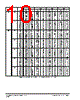


I. Device Families & Types
️· MMBR941: Part of the series. A Bipolar Junction Transistor (BJT). Appears to have a specific 'T3' variant referenced.
️· MRF947: Part of the series. Another BJT.
️· MRF9411: Part of the series. Another BJT.
II. General Characteristics (Common to the Series, as indicated)
️· RF Devices: All are designed for RF applications.
️· Function: These are likely designed as amplifier or RF front-end components.
️· SF (Signal Function): 'SF – 11N < 1 GHz', 'SF – 31IN ≥ 1 GHz'. Implies different operational frequencies for different applications or configurations.
️· VCE = 6V: The collector-emitter voltage is 6 volts.
III. Figures & Associated Data Points
Let's categorize data from the figures, noting what we can decipher. Note some figures are challenging to read exact values from.
️· Figure 1 (General): Illustrates a functional circuit schematic (all devices).
️· Figure 10 (Capacitance vs Voltage): Shows the capacitance characteristics of the devices as a function of voltage. It's a plot of capacitance changing with applied voltage.
️· Figure 11 (DC Current Gain vs Collector Current): This figure illustrates how the device's current gain changes with the collector current. It shows a typical characteristic curve for a BJT.
️· Figure 12 (Gain–Bandwidth Product vs Collector Current): Demonstrates the relationship between the gain-bandwidth product and the collector current.
️· Figure 13 (Associated Gain and Minimum Noise Figure vs Collector Current): Shows how the forward insertion gain and the minimum noise figure change with the collector current.
️· Figure 14 (Forward Insertion Gain and Maximum Stable/Available Power Gain vs Frequency): Illustrates the forward insertion gain and maximum available power gain as a function of frequency.
️· Noise Figure: Minimum Noise Figure is demonstrated in Figure 13. NFm = 'noise figure'. 'MSG' and 'MAG' terms are shown; these are possibly associated with the gain characteristics.
️· S21: Likely a representation of transmission coefficient.
IV. Important Values & Relationships (Estimated from figures)
️· Current Gain: Shows a rise in current gain with increasing collector current.
️· Gain-Bandwidth: Generally increases with increasing collector current.
️· Noise Figure: Exhibits a minimum noise figure at specific collector current levels.
️· Gain vs. Frequency: Forward gain decreases with increasing frequency.
️· Stable Power Gain: Demonstrates how maximum power gain depends on frequency and the power characteristics.
️· IC = 5 mA: A current value used in one of the figures (Figure 2, possibly).
V. Notes & Caveats
️· Image Quality: The image resolution affects the ability to read exact values from the figures.
️· Missing Context: Without more information, specific design parameters or application notes are unavailable.
️· Abbreviations: Several abbreviations are used without full explanation (e.g., "SF", "MSG", "MAG").
I. Device Families & Types
️· MMBR941: Part of the series. A Bipolar Junction Transistor (BJT). Appears to have a specific 'T3' variant referenced.
️· MRF947: Part of the series. Another BJT.
️· MRF9411: Part of the series. Another BJT.
II. General Characteristics (Common to the Series, as indicated)
️· RF Devices: All are designed for RF applications.
️· Function: These are likely designed as amplifier or RF front-end components.
️· SF (Signal Function): 'SF – 11N < 1 GHz', 'SF – 31IN ≥ 1 GHz'. Implies different operational frequencies for different applications or configurations.
️· VCE = 6V: The collector-emitter voltage is 6 volts.
III. Figures & Associated Data Points
Let's categorize data from the figures, noting what we can decipher. Note some figures are challenging to read exact values from.
️· Figure 1 (General): Illustrates a functional circuit schematic (all devices).
️· Figure 10 (Capacitance vs Voltage): Shows the capacitance characteristics of the devices as a function of voltage. It's a plot of capacitance changing with applied voltage.
️· Figure 11 (DC Current Gain vs Collector Current): This figure illustrates how the device's current gain changes with the collector current. It shows a typical characteristic curve for a BJT.
️· Figure 12 (Gain–Bandwidth Product vs Collector Current): Demonstrates the relationship between the gain-bandwidth product and the collector current.
️· Figure 13 (Associated Gain and Minimum Noise Figure vs Collector Current): Shows how the forward insertion gain and the minimum noise figure change with the collector current.
️· Figure 14 (Forward Insertion Gain and Maximum Stable/Available Power Gain vs Frequency): Illustrates the forward insertion gain and maximum available power gain as a function of frequency.
️· Noise Figure: Minimum Noise Figure is demonstrated in Figure 13. NFm = 'noise figure'. 'MSG' and 'MAG' terms are shown; these are possibly associated with the gain characteristics.
️· S21: Likely a representation of transmission coefficient.
IV. Important Values & Relationships (Estimated from figures)
️· Current Gain: Shows a rise in current gain with increasing collector current.
️· Gain-Bandwidth: Generally increases with increasing collector current.
️· Noise Figure: Exhibits a minimum noise figure at specific collector current levels.
️· Gain vs. Frequency: Forward gain decreases with increasing frequency.
️· Stable Power Gain: Demonstrates how maximum power gain depends on frequency and the power characteristics.
️· IC = 5 mA: A current value used in one of the figures (Figure 2, possibly).
V. Notes & Caveats
️· Image Quality: The image resolution affects the ability to read exact values from the figures.
️· Missing Context: Without more information, specific design parameters or application notes are unavailable.
️· Abbreviations: Several abbreviations are used without full explanation (e.g., "SF", "MSG", "MAG").
| Part No. | MMBR941LT1 |
| Manufacturer | MOTOROLA |
| Size | 309 Kbytes |
| Pages | 17 pages |
| Description | NPN Silicon Low Noise, High-Frequency Transistors |
| Does ALLDATASHEET help your business so far? [ DONATE ] |
About Alldatasheet | Advertisement | Contact us | Privacy Policy | Link to Datasheet | Link Exchange | Manufacturer List All Rights Reserved©Alldatasheet.com |
| Russian : Alldatasheetru.com | Korean : Alldatasheet.co.kr | Spanish : Alldatasheet.es | French : Alldatasheet.fr | Italian : Alldatasheetit.com Portuguese : Alldatasheetpt.com | Polish : Alldatasheet.pl | Vietnamese : Alldatasheet.vn Indian : Alldatasheet.in | Mexican : Alldatasheet.com.mx | British : Alldatasheet.co.uk | New Zealand : Alldatasheet.co.nz |
|
Family Site : ic2ic.com |
icmetro.com |
 New Zealand ▼
  English
 Chinese
 German
 Japanese
 Russian
 Korean
 Spanish
 French
 Italian
 Portuguese
 Polish
 Vietnamese
 Indian
 Mexican
 British