|
Electronic Components Datasheet Search |
|
|
Electronic Components Datasheet Search |
|
H8SX/1663R Datasheet(PDF) 375 Page - Renesas Technology Corp |
|
|
|||||||||||||||||||||||||||||
H8SX/1663R Datasheet(HTML) 375 Page - Renesas Technology Corp |
|
|
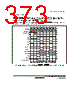
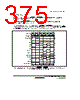
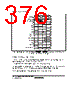
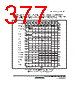
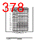
375 / 1504 page 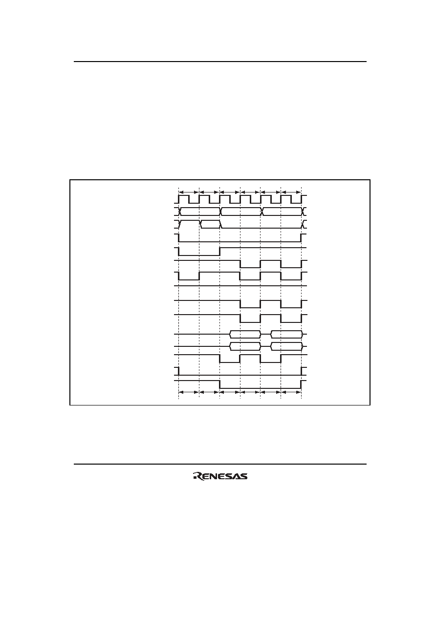 Section 9 Bus Controller (BSC) Rev. 2.00 Sep. 24, 2008 Page 343 of 1468 REJ09B0412-0200 (5) When DKC = 1 With DKC = 1 or EDKC = 1, the DACK and EDACK signals are asserted a half cycle earlier compared to the case when DKC = 0 or EDKC = 0. In fast-page access, the DACK signal continues to be low. In this case, bus cycles can be distinguished by the BS output timing. Figure 9.89 shows an output timing example of the DACK and EDACK signals when DKC = 1 or EDKC = 1, and DDS = 1 or EDDS = 1. Figure 9.90 shows an output timing example of the DACK and EDACK signals when DKC = 1 or EDKC = 1, and DDS = 0 or EDDS = 0. T p T r T c1 T c2 T c1 T c2 Address bus Row address Column address 2 Column address 1 SDRAM φ CS Precharge-sel RAS CAS WE CKE PALL ACTV NOP NOP WRIT WRIT DQMLU DQMLL D7 to D0 BS DACK or EDACK RD/ WR D15 to D8 Row address High Figure 9.89 Output Timing Example of DACK and EDACK when DKC = 1 or EDKC = 1 and DDS = 1 or EDDS = 1 (Write) |
|
Link URL |
| Does ALLDATASHEET help your business so far? [ DONATE ] |
About Alldatasheet | Advertisement | Contact us | Privacy Policy | Link to Datasheet | Link Exchange | Manufacturer List All Rights Reserved©Alldatasheet.com |
| Russian : Alldatasheetru.com | Korean : Alldatasheet.co.kr | Spanish : Alldatasheet.es | French : Alldatasheet.fr | Italian : Alldatasheetit.com Portuguese : Alldatasheetpt.com | Polish : Alldatasheet.pl | Vietnamese : Alldatasheet.vn Indian : Alldatasheet.in | Mexican : Alldatasheet.com.mx | British : Alldatasheet.co.uk | New Zealand : Alldatasheet.co.nz |
|
Family Site : ic2ic.com |
icmetro.com |
 New Zealand ▼
 English
 Chinese
 German
 Japanese
 Russian
 Korean
 Spanish
 French
 Italian
 Portuguese
 Polish
 Vietnamese
 Indian
 Mexican
 British
 New Zealand