|
Electronic Components Datasheet Search |
|
|
Electronic Components Datasheet Search |
|
H8SX/1663M Datasheet(PDF) 317 Page - Renesas Technology Corp |
|
|
|||||||||||||||||||||||||||||
H8SX/1663M Datasheet(HTML) 317 Page - Renesas Technology Corp |
|
|
317 / 1504 page 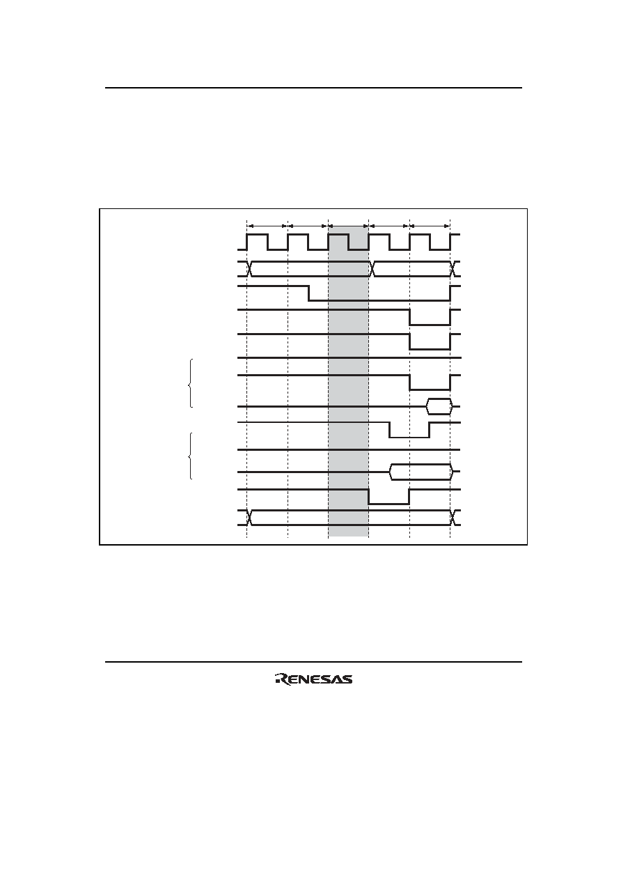 Section 9 Bus Controller (BSC) Rev. 2.00 Sep. 24, 2008 Page 285 of 1468 REJ09B0412-0200 To ensure the row address hold time or read access time, one to three of Trw cycles in which the row address output is retained can be inserted between the Tr and Tc1 cycles. The RAS signal is driven low in the Tr cycle and the column address is output in the Tc1 cycle. Set the bit according to the DRAM to be used and the frequency of this LSI so that the row address hold time to the rising edge of the RAS signal is ensured. Figure 9.41 shows an access timing example when one Trw cycle is specified. T p T r T rw T c1 T c2 Address bus Row address Column address B φ RAS LUCAS LLCAS WE OE (RD) WE OE (RD) Data bus High High Read Write Data bus BS RD/ WR Figure 9.41 Access Timing Example when One Trw Cycle is Specified (RAST=0, CAST=0) |
|
Link URL |
| Does ALLDATASHEET help your business so far? [ DONATE ] |
About Alldatasheet | Advertisement | Contact us | Privacy Policy | Link to Datasheet | Link Exchange | Manufacturer List All Rights Reserved©Alldatasheet.com |
| Russian : Alldatasheetru.com | Korean : Alldatasheet.co.kr | Spanish : Alldatasheet.es | French : Alldatasheet.fr | Italian : Alldatasheetit.com Portuguese : Alldatasheetpt.com | Polish : Alldatasheet.pl | Vietnamese : Alldatasheet.vn Indian : Alldatasheet.in | Mexican : Alldatasheet.com.mx | British : Alldatasheet.co.uk | New Zealand : Alldatasheet.co.nz |
|
Family Site : ic2ic.com |
icmetro.com |
 New Zealand ▼
 English
 Chinese
 German
 Japanese
 Russian
 Korean
 Spanish
 French
 Italian
 Portuguese
 Polish
 Vietnamese
 Indian
 Mexican
 British
 New Zealand