|
Electronic Components Datasheet Search |
|
|
Electronic Components Datasheet Search |
|
HMC674LC3CTR-R5 Datasheet(PDF) 11 Page - Analog Devices |
|
|
|||||||||||||||||||||||||||||
HMC674LC3CTR-R5 Datasheet(HTML) 11 Page - Analog Devices |
|
|
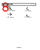
11 / 14 page 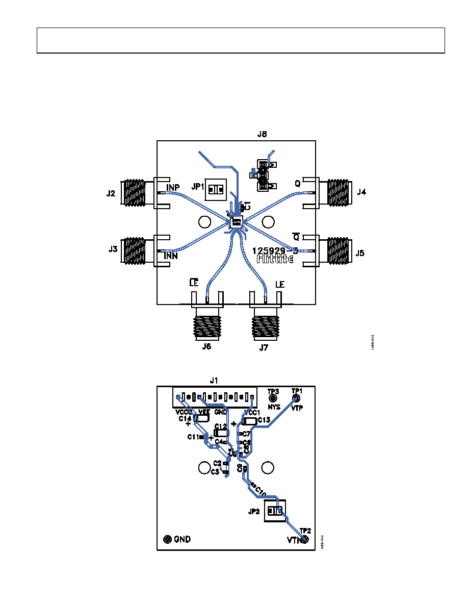 Data Sheet HMC674LC3C/HMC674LP3E Rev. K | Page 11 of 14 APPLICATIONS INFORMATION EVALUATION PRINTED CIRCUIT BOARD (PCB) Figure 13 shows the front side of the evaluation PCB, and Figure 14 shows the back side of the evaluation PCB. The evaluation PCB used in the application must use RF circuit design techniques. Signal lines must have 50 Ω impedance, and the package ground leads must be connected directly to the ground plane similar to that shown in Figure 15. Use a sufficient number of via holes to connect the top and bottom ground planes to provide good RF grounding to 10 GHz. The evaluation PCB shown in Figure 13 is available from Analog Devices, Inc., upon request. Figure 13. Front Side of the Evaluation PCB Figure 14. Back Side of the Evaluation PCB |
|
|
Link URL |
| Does ALLDATASHEET help your business so far? [ DONATE ] |
About Alldatasheet | Advertisement | Contact us | Privacy Policy | Link to Datasheet | Link Exchange | Manufacturer List All Rights Reserved©Alldatasheet.com |
| Russian : Alldatasheetru.com | Korean : Alldatasheet.co.kr | Spanish : Alldatasheet.es | French : Alldatasheet.fr | Italian : Alldatasheetit.com Portuguese : Alldatasheetpt.com | Polish : Alldatasheet.pl | Vietnamese : Alldatasheet.vn Indian : Alldatasheet.in | Mexican : Alldatasheet.com.mx | British : Alldatasheet.co.uk | New Zealand : Alldatasheet.co.nz |
|
Family Site : ic2ic.com |
icmetro.com |
 New Zealand ▼
 English
 Chinese
 German
 Japanese
 Russian
 Korean
 Spanish
 French
 Italian
 Portuguese
 Polish
 Vietnamese
 Indian
 Mexican
 British
 New Zealand