|
Electronic Components Datasheet Search |
|
|
Electronic Components Datasheet Search |
|
INMP401ACEZ-R7 Datasheet(PDF) 10 Page - TDK Electronics |
|
|
|||||||||||||||||||||||||||||
INMP401ACEZ-R7 Datasheet(HTML) 10 Page - TDK Electronics |
|
|
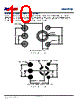
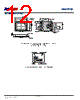
10 / 14 page 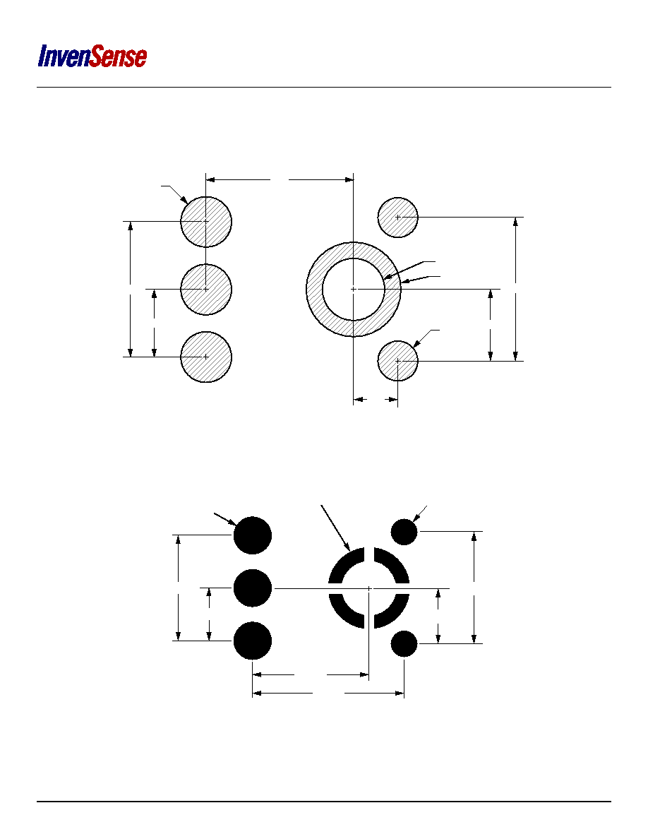 INMP401 PCB DESIGN AND LAND PATTERN LAYOUT The recommended PCB land pattern for the INMP401 should be laid out to a 1:1 ratio to the solder pads on the microphone package, as shown in Figure 8. Take care to avoid applying solder paste to the sound hole in the PCB. A suggested solder paste stencil pattern layout is shown in Figure 9. The diameter of the sound hole in the PCB should be larger than the diameter of the sound port of the microphone. A minimum diameter of 0.5 mm is recommended. Figure 8. PCB Land Pattern Layout Dimensions shown in millimeters Figure 9. Suggested Solder Paste Stencil Pattern Layout Dimensions shown in millimeters 2.62 ø1.10 ø1.68 ø0.70 (2×) ø0.90 (3×) 2.40 1.20 2.54 0.79 1.27 1.27mm 1.2mm 2.54mm 2.62mm 3.41mm 2.4mm 0.85mm DIA. (3×) 1.8mm/1.3mm DIA. 0.2032 CUT WIDTH (4×) 0.649mm DIA. (2×) Page 10 of 14 Document Number: DS-INMP401-00 Revision: 1.0. |
|
|
Link URL |
| Does ALLDATASHEET help your business so far? [ DONATE ] |
About Alldatasheet | Advertisement | Contact us | Privacy Policy | Link to Datasheet | Link Exchange | Manufacturer List All Rights Reserved©Alldatasheet.com |
| Russian : Alldatasheetru.com | Korean : Alldatasheet.co.kr | Spanish : Alldatasheet.es | French : Alldatasheet.fr | Italian : Alldatasheetit.com Portuguese : Alldatasheetpt.com | Polish : Alldatasheet.pl | Vietnamese : Alldatasheet.vn Indian : Alldatasheet.in | Mexican : Alldatasheet.com.mx | British : Alldatasheet.co.uk | New Zealand : Alldatasheet.co.nz |
|
Family Site : ic2ic.com |
icmetro.com |
 New Zealand ▼
 English
 Chinese
 German
 Japanese
 Russian
 Korean
 Spanish
 French
 Italian
 Portuguese
 Polish
 Vietnamese
 Indian
 Mexican
 British
 New Zealand