|
Electronic Components Datasheet Search |
|
|
Electronic Components Datasheet Search |
|
FP1110V1-R22-R Datasheet(PDF) 2 Page - Eaton All Rights Reserved. |
|
|
|||||||||||||||||||||||||||||
FP1110V1-R22-R Datasheet(HTML) 2 Page - Eaton All Rights Reserved. |
|
|
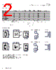
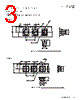
2 / 6 page 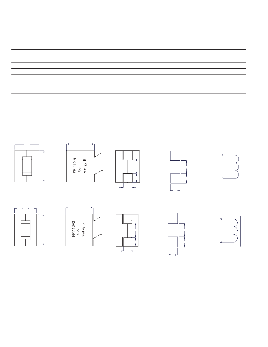 2 Technical Data 10427 Effective August 2015 FP1110V High frequency, high current power inductors www.eaton.com/elx Product specifications Part Number7 OCL1 (nH) ±10% FLL2 minimum (nH) Irms3 (amps) Isat14 (amps) Isat25 (amps) DCR (mΩ) ±5% @ +20°C K-factor6 V1-10.7 x 7.5 x 9.5mm FP1110V1-R20-R 195 140 61 70 58 0.23 278 FP1110V1-R22-R 220 158 61 64 51 0.23 278 FP1110V1-R27-R 270 173 61 55 44 0.23 278 FP1110V1-R32-R 320 230 61 42 34 0.23 278 V2-10.5 x 6.2 x 9.5mm FP1110V2-R200-R 200 144 61 65 52 0.18 328 1. Open Circuit Inductance (OCL) Test Parameters: 100kHz, 0.1Vrms, 0.0Adc, +25°C 2. Full Load Inductance (FLL) Test Parameters: 100kHz, 0.1Vrms, @ I sat1, @ +25ºC 3. Irms: DC current for an approximate temperature rise of 40°C without core loss. Derating is necessary for AC currents. PCB layout, trace thickness and width, air-flow, and proximity of other heat generating components will affect the temperature rise. It is recommended that the temperature of the part not exceed +125°C under worst case operating conditions verified in the end application. 4. I sat1 : Peak current for approximately 20% rolloff @ +25ºC 5. Isat : Peak current for approximately 20% rolloff @ +100ºC 6. K-factor: Used to determine B p-p for core loss (see graph). Bp-p = K * L * ΔI * 10 -3 . B p-p:(Gauss), K: (K-factor from table), L: (Inductance in nH), ΔI (Peak to peak ripple current in Amps). 7. Part Number Definition: FP1110Vx-Rxx(x)-R FP1110V = Product code x= DCR indicator Rxx(x)= Inductance value in uH, R= decimal point -R suffix = RoHS compliant Dimensions (mm) Part marking: FP1110V1 or V2, Rxx(x)=inductance value in µH, R=decimal point wwllyy= date code, R=revision level DCR measured from point “a” to point “b” Soldering surfaces to be coplanar within 0.10 millimeters Do not route traces or vias underneath the inductor. Recommended Pad Layout Schematic Recommended Pad Layout Schematic 7.5 max 9.5 max 10.7 max a b 4.6 2.8 2.8 4.1 3.4 3.3 10.5 max 6.2 max 9.5 max a b 4.2 2.15 3.0 4.0 3.6 2.8 |
|
|
Link URL |
| Does ALLDATASHEET help your business so far? [ DONATE ] |
About Alldatasheet | Advertisement | Contact us | Privacy Policy | Link to Datasheet | Link Exchange | Manufacturer List All Rights Reserved©Alldatasheet.com |
| Russian : Alldatasheetru.com | Korean : Alldatasheet.co.kr | Spanish : Alldatasheet.es | French : Alldatasheet.fr | Italian : Alldatasheetit.com Portuguese : Alldatasheetpt.com | Polish : Alldatasheet.pl | Vietnamese : Alldatasheet.vn Indian : Alldatasheet.in | Mexican : Alldatasheet.com.mx | British : Alldatasheet.co.uk | New Zealand : Alldatasheet.co.nz |
|
Family Site : ic2ic.com |
icmetro.com |
 New Zealand ▼
 English
 Chinese
 German
 Japanese
 Russian
 Korean
 Spanish
 French
 Italian
 Portuguese
 Polish
 Vietnamese
 Indian
 Mexican
 British
 New Zealand