 |
Electronic Components Datasheet Search |
|
|
Electronic Components Datasheet Search |
|
IS25LP016D-RKLE:P Datasheet(PDF) 53 Page - Integrated Silicon Solution, Inc |
|
|
|||||||||||||||||||||||||||||
IS25LP016D-RKLE:P Datasheet(HTML) 53 Page - Integrated Silicon Solution, Inc |
|
|
53 / 114 page 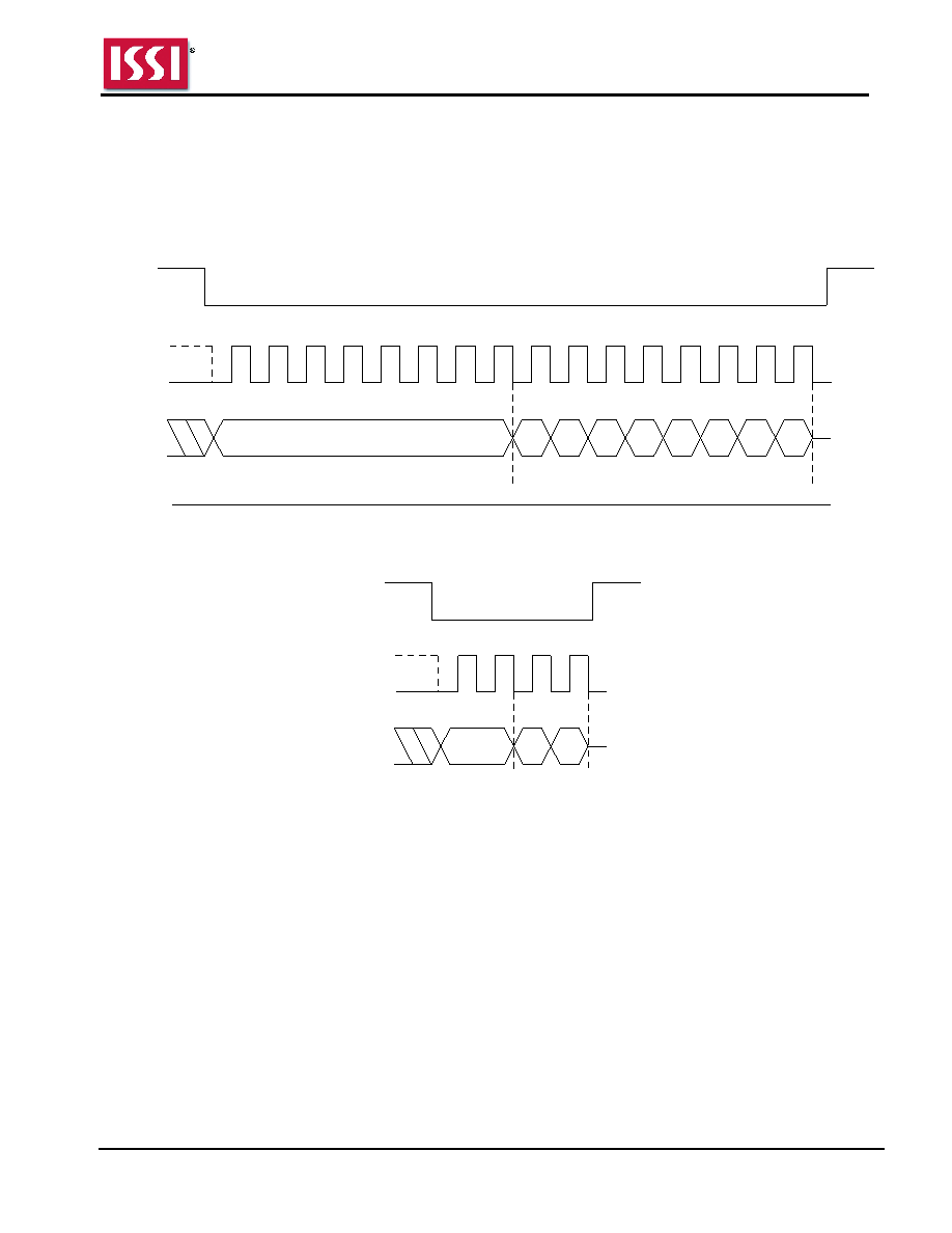 IS25LP016D IS25WP016D Integrated Silicon Solution, Inc.- www.issi.com 53 Rev. B10 03/09/2020 8.17 WRITE STATUS REGISTER OPERATION (WRSR, 01h) The Write Status Register (WRSR) instruction allows the user to enable or disable the block protection and Status Register write protection features by writing “0”s or “1”s into the non-volatile BP3, BP2, BP1, BP0, and SRWD bits. Also WRSR instruction allows the user to disable or enable quad operation by writing “0” or “1” into the non-volatile QE bit. Figure 8.28 Write Status Register Sequence In SPI Mode Instruction = 01h CE # SCK SI SO Data In 0 1 2 3 4 5 6 7 8 9 10 11 12 13 14 15 Mode 3 Mode 0 7 3 2 1 0 6 5 4 High Impedence Figure 8.29 Write Status Register Sequence In QPI Mode 01h 0 1 Mode 3 Mode 0 2 3 7:4 3:0 CE# SCK IO[3:0] Data In |
|
Link URL |
| Does ALLDATASHEET help your business so far? [ DONATE ] |
About Alldatasheet | Advertisement | Contact us | Privacy Policy | Link to Datasheet | Link Exchange | Manufacturer List All Rights Reserved©Alldatasheet.com |
| Russian : Alldatasheetru.com | Korean : Alldatasheet.co.kr | Spanish : Alldatasheet.es | French : Alldatasheet.fr | Italian : Alldatasheetit.com Portuguese : Alldatasheetpt.com | Polish : Alldatasheet.pl | Vietnamese : Alldatasheet.vn Indian : Alldatasheet.in | Mexican : Alldatasheet.com.mx | British : Alldatasheet.co.uk | New Zealand : Alldatasheet.co.nz |
|
Family Site : ic2ic.com |
icmetro.com |
 New Zealand ▼
 English
 Chinese
 German
 Japanese
 Russian
 Korean
 Spanish
 French
 Italian
 Portuguese
 Polish
 Vietnamese
 Indian
 Mexican
 British
 New Zealand


