|
Electronic Components Datasheet Search |
|
|
Electronic Components Datasheet Search |
|
PLL102-10SC-R Datasheet(PDF) 1 Page - PhaseLink Corporation |
|
|
|||||||||||||||||||||||||||||
PLL102-10SC-R Datasheet(HTML) 1 Page - PhaseLink Corporation |
|
|
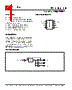
1 / 6 page 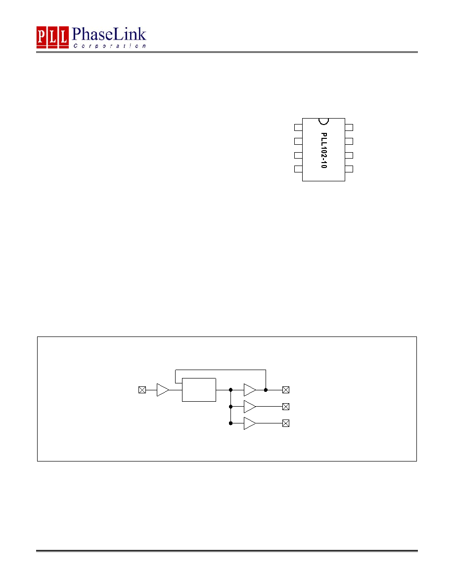 PLL102-10 Low Skew Output Buffer 47745 Fremont Blvd., Fremont, California 94538 Tel (510) 492-0990 Fax (510) 492-0991 www.phaselink.com Rev 03/22/05 Page 1 FEATURES • Frequency range 50 ~ 120MHz. • Internal phase locked loop will allow spread spec- trum modulation on reference clock to pass to out- puts. • Zero input - output delay. • Less than 700 ps device - device skew. • Less than 250 ps skew between outputs. • Less than 100 ps cycle - cycle jitter. • 2.5V or 3.3V power supply operation. • Available in 8-Pin SOIC or MSOP package. DESCRIPTION The PLL102-10 is a high performance, low skew, low jitter zero delay buffer designed to distribute high speed clocks and is available in 8-pin SOIC or MSOP package. It has two outputs that are synchronized with the input. The synchronization is established via CLKOUT feed back to the input of the PLL. Since the skew between the input and output is less than ±350 ps, the device acts as a zero delay buffer. PIN CONFIGURATION BLOCK DIAGRAM 1 2 3 4 5 6 7 8 REFIN GND CLK1 CLK2 CLKOUT DNC VDD DNC PLL REFIN CLKOUT CLK1 CLK2 |
Similar Part No. - PLL102-10SC-R |
|
Similar Description - PLL102-10SC-R |
|
|
|
Link URL |
| Does ALLDATASHEET help your business so far? [ DONATE ] |
About Alldatasheet | Advertisement | Contact us | Privacy Policy | Link to Datasheet | Link Exchange | Manufacturer List All Rights Reserved©Alldatasheet.com |
| Russian : Alldatasheetru.com | Korean : Alldatasheet.co.kr | Spanish : Alldatasheet.es | French : Alldatasheet.fr | Italian : Alldatasheetit.com Portuguese : Alldatasheetpt.com | Polish : Alldatasheet.pl | Vietnamese : Alldatasheet.vn Indian : Alldatasheet.in | Mexican : Alldatasheet.com.mx | British : Alldatasheet.co.uk | New Zealand : Alldatasheet.co.nz |
|
Family Site : ic2ic.com |
icmetro.com |
 New Zealand ▼
 English
 Chinese
 German
 Japanese
 Russian
 Korean
 Spanish
 French
 Italian
 Portuguese
 Polish
 Vietnamese
 Indian
 Mexican
 British
 New Zealand