 |
Electronic Components Datasheet Search |
|
|
Electronic Components Datasheet Search |
|
ADCA5190ACPZ-R7 Datasheet(PDF) 21 Page - Analog Devices |
|
|
|||||||||||||||||||||||||||||
ADCA5190ACPZ-R7 Datasheet(HTML) 21 Page - Analog Devices |
|
|
21 / 22 page 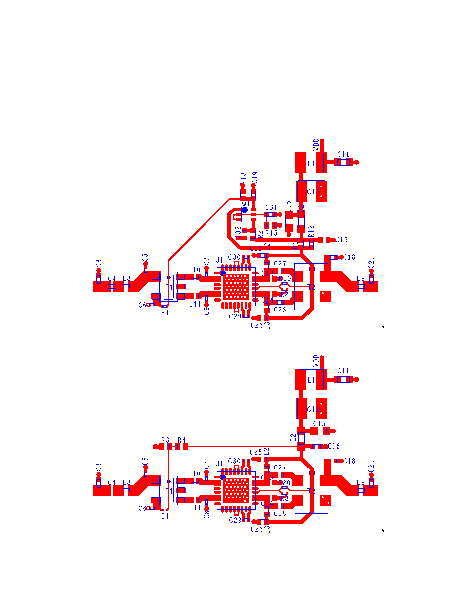 Data Sheet ADCA5190 APPLICATIONS INFORMATION analog.com Rev. 0 | 21 of 22 LAYOUT CONSIDERATIONS The layouts in Figure 33 and Figure 34 are similar to that used in the evaluation circuit for the ADCA5190. When deviating from this recommended layout, keep the following points in mind: ► All RF components must be kept as close as possible to the ADCA5190. These components include the transformers and all tuning components in series or shunt to the RF traces. ► Symmetry must be strictly maintained between the input and output balun. ► C29 and C30, the feedback capacitors, must be kept as close as possible to the ADCA5190 and must be referenced to the RF ground plane. ► Components around Q1 must be kept physically close to the ADCA5190. Figure 33. Suggested Downstream CATV Application Circuit with Active Biasing Layout Figure 34. Suggested Downstream CATV Application Circuit with Passive Biasing Layout |
|
|
Link URL |
| Does ALLDATASHEET help your business so far? [ DONATE ] |
About Alldatasheet | Advertisement | Contact us | Privacy Policy | Link to Datasheet | Link Exchange | Manufacturer List All Rights Reserved©Alldatasheet.com |
| Russian : Alldatasheetru.com | Korean : Alldatasheet.co.kr | Spanish : Alldatasheet.es | French : Alldatasheet.fr | Italian : Alldatasheetit.com Portuguese : Alldatasheetpt.com | Polish : Alldatasheet.pl | Vietnamese : Alldatasheet.vn Indian : Alldatasheet.in | Mexican : Alldatasheet.com.mx | British : Alldatasheet.co.uk | New Zealand : Alldatasheet.co.nz |
|
Family Site : ic2ic.com |
icmetro.com |
 New Zealand ▼
 English
 Chinese
 German
 Japanese
 Russian
 Korean
 Spanish
 French
 Italian
 Portuguese
 Polish
 Vietnamese
 Indian
 Mexican
 British
 New Zealand


