 |
Electronic Components Datasheet Search |
|
|
Electronic Components Datasheet Search |
|
SCD42-D-R2 Datasheet(PDF) 18 Page - Sensirion AG Switzerland |
|
|
|||||||||||||||||||||||||||||
SCD42-D-R2 Datasheet(HTML) 18 Page - Sensirion AG Switzerland |
|
|
18 / 21 page 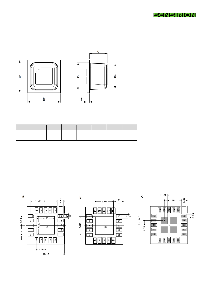 www.sensirion.com Version 1 – March 2022 18/21 4 Mechanical specifications 4.1 Package Outline Figure 3 schematically displays the package outline. The notched corner of the protection membrane serves as a polarity mark to indicate pin 1 location. Nominal dimensions and tolerances are listed in Table 27. Figure 3: Packaging outline drawing of the SCD42: (left) top view and (right) side view. Nominal dimensions and tolerances are listed in millimeters. Dimension a b c d e f Nominal [mm] 10.1 10.1 8.5 7.8 5.5 0.8 Tolerance [mm] ± 0.3 ± 0.3 ± 0.2 ± 0.2 ± 0.3 ± 0.2 Table 27: Nominal dimensions and tolerances SCD42 (all in mm). The weight of the sensor is approx. 0.6 g. Note that the white protection membrane on top of the sensor must not be removed or tampered with to ensure proper sensor operation. 4.2 Land Pattern Recommended land pattern, solder paste and solder mask are shown in Figure 4. These are recommendations only and not specifications. The exact mask geometries, distances and stencil thicknesses must be adapted to the customer soldering processes. Figure 4: SCD42 footprint (top view): landing pads (a), solder mask (b) and solder paste (c). |
|
|
Link URL |
| Does ALLDATASHEET help your business so far? [ DONATE ] |
About Alldatasheet | Advertisement | Contact us | Privacy Policy | Link to Datasheet | Link Exchange | Manufacturer List All Rights Reserved©Alldatasheet.com |
| Russian : Alldatasheetru.com | Korean : Alldatasheet.co.kr | Spanish : Alldatasheet.es | French : Alldatasheet.fr | Italian : Alldatasheetit.com Portuguese : Alldatasheetpt.com | Polish : Alldatasheet.pl | Vietnamese : Alldatasheet.vn Indian : Alldatasheet.in | Mexican : Alldatasheet.com.mx | British : Alldatasheet.co.uk | New Zealand : Alldatasheet.co.nz |
|
Family Site : ic2ic.com |
icmetro.com |
 New Zealand ▼
 English
 Chinese
 German
 Japanese
 Russian
 Korean
 Spanish
 French
 Italian
 Portuguese
 Polish
 Vietnamese
 Indian
 Mexican
 British
 New Zealand


