|
Electronic Components Datasheet Search |
|
|
Electronic Components Datasheet Search |
|
ADL5306ACP-R2 Datasheet(PDF) 5 Page - Analog Devices |
|
|
|||||||||||||||||||||||||||||
ADL5306ACP-R2 Datasheet(HTML) 5 Page - Analog Devices |
|
|
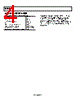
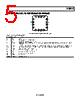
5 / 16 page 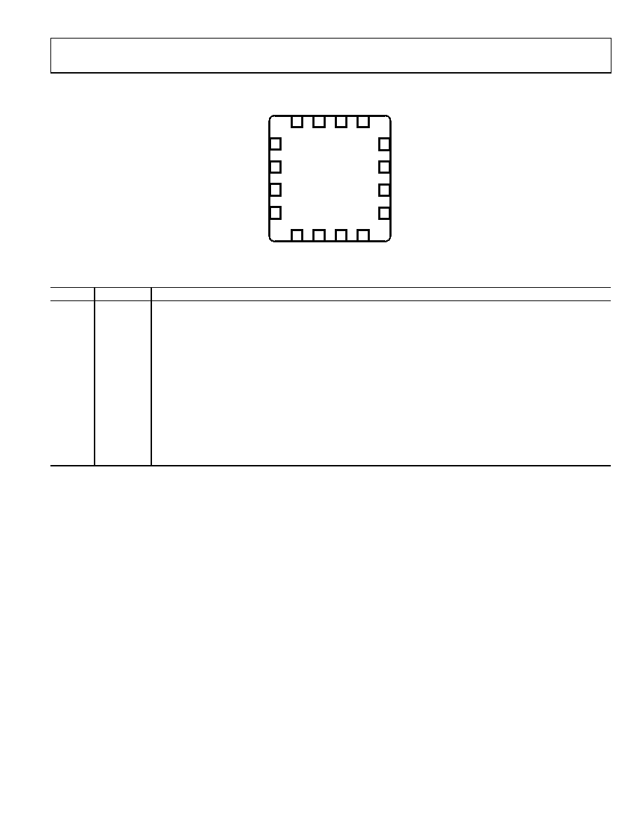 ADL5306 PIN CONFIGURATION AND PIN FUNCTION DESCRIPTIONS NC INPT VREF IREF SCAL BFIN COMM COMM COMM VPOS COMM VNEG VNEG VSUM VOUT VLOG 1 2 3 4 56 7 8 9 10 11 12 13 14 15 16 ADL5306 03727-0-002 Figure 2. 16-Lead Leadframe Chip Scale Package (LFCSP) Table 3. Pin Function Descriptions Pin No. Mnemonic Function 1 NC N/A 2 VREF Reference Output Voltage of 2.5 V. 3 IREF Accepts (Sinks) Reference Current IREF. 4 INPT Accepts (Sinks) Photodiode Current IPD. Usually connected to photodiode anode such that photocurrent flows into INPT. 5 VSUM Guard Pin. Used to shield the INPT current line and for optional adjustment of the INPT and IREF node potential. 6, 7 VNEG Optional Negative Supply, VN. This pin is usually grounded; for details of usage, see the Applications section. 8 VPOS Positive Supply, ( VP – VN ) ≤ 11 V. 9 VLOG Output of the Logarithmic Front End. 10 BFIN Buffer Amplifier Noninverting Input. 11 SCAL Buffer Amplifier Inverting Input. 12 VOUT Buffer Output. 13–16 COMM Analog Ground. Rev. 0 | Page 5 of 16 |
|
|
Link URL |
| Does ALLDATASHEET help your business so far? [ DONATE ] |
About Alldatasheet | Advertisement | Contact us | Privacy Policy | Link to Datasheet | Link Exchange | Manufacturer List All Rights Reserved©Alldatasheet.com |
| Russian : Alldatasheetru.com | Korean : Alldatasheet.co.kr | Spanish : Alldatasheet.es | French : Alldatasheet.fr | Italian : Alldatasheetit.com Portuguese : Alldatasheetpt.com | Polish : Alldatasheet.pl | Vietnamese : Alldatasheet.vn Indian : Alldatasheet.in | Mexican : Alldatasheet.com.mx | British : Alldatasheet.co.uk | New Zealand : Alldatasheet.co.nz |
|
Family Site : ic2ic.com |
icmetro.com |
 New Zealand ▼
 English
 Chinese
 German
 Japanese
 Russian
 Korean
 Spanish
 French
 Italian
 Portuguese
 Polish
 Vietnamese
 Indian
 Mexican
 British
 New Zealand