|
Electronic Components Datasheet Search |
|
|
Electronic Components Datasheet Search |
|
ADP1611ARMZ-R7 Datasheet(PDF) 16 Page - Analog Devices |
|
|
|||||||||||||||||||||||||||||
ADP1611ARMZ-R7 Datasheet(HTML) 16 Page - Analog Devices |
|
|
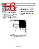
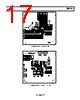
16 / 20 page 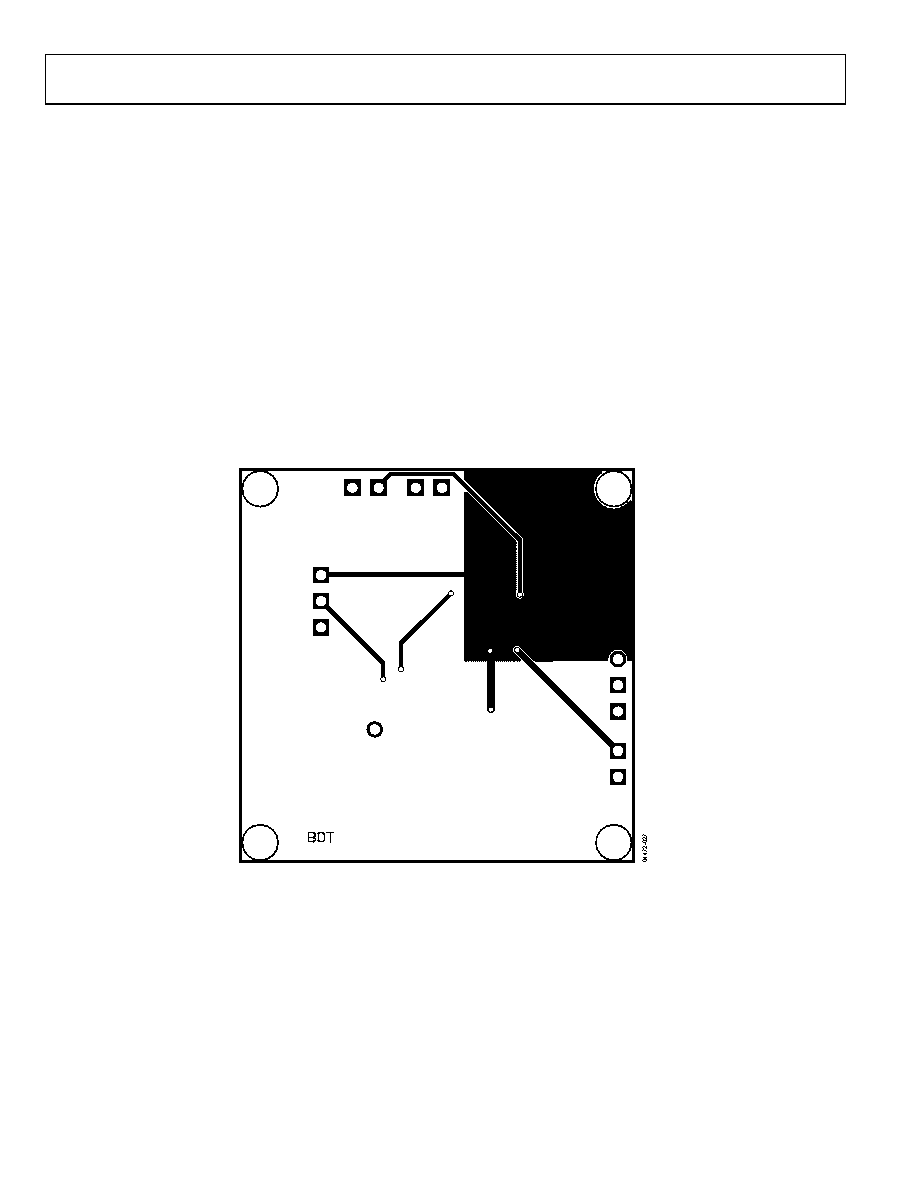 ADP1611 Rev. 0 | Page 16 of 20 LAYOUT PROCEDURE To achieve high efficiency, good regulation, and stability, a well- designed printed circuit board layout is required. Where possible, use the sample application board layout as a model. Follow these guidelines when designing printed circuit boards (see Figure 1): • Keep the low ESR input capacitor, CIN, close to IN and GND. • Keep the high current path from CIN through the inductor, L1, to SW and PGND as short as possible. • Keep the high current path from CIN through L1, the rectifier, D1, and the output capacitor, COUT, as short as possible. • Keep high current traces as short and as wide as possible. • Place the feedback resistors as close to FB as possible to prevent noise pickup. • Place the compensation components as close as possible to COMP. • Avoid routing high impedance traces near any node connected to SW or near the inductor to prevent radiated noise injection. Figure 31. Sample Application Board (Bottom Layer) |
|
|
Link URL |
| Does ALLDATASHEET help your business so far? [ DONATE ] |
About Alldatasheet | Advertisement | Contact us | Privacy Policy | Link to Datasheet | Link Exchange | Manufacturer List All Rights Reserved©Alldatasheet.com |
| Russian : Alldatasheetru.com | Korean : Alldatasheet.co.kr | Spanish : Alldatasheet.es | French : Alldatasheet.fr | Italian : Alldatasheetit.com Portuguese : Alldatasheetpt.com | Polish : Alldatasheet.pl | Vietnamese : Alldatasheet.vn Indian : Alldatasheet.in | Mexican : Alldatasheet.com.mx | British : Alldatasheet.co.uk | New Zealand : Alldatasheet.co.nz |
|
Family Site : ic2ic.com |
icmetro.com |
 New Zealand ▼
 English
 Chinese
 German
 Japanese
 Russian
 Korean
 Spanish
 French
 Italian
 Portuguese
 Polish
 Vietnamese
 Indian
 Mexican
 British
 New Zealand