|
Electronic Components Datasheet Search |
|
|
Electronic Components Datasheet Search |
|
SE2525L-R Datasheet(PDF) 3 Page - SiGe Semiconductor, Inc. |
|
|
|||||||||||||||||||||||||||||
SE2525L-R Datasheet(HTML) 3 Page - SiGe Semiconductor, Inc. |
|
|
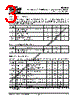
3 / 12 page 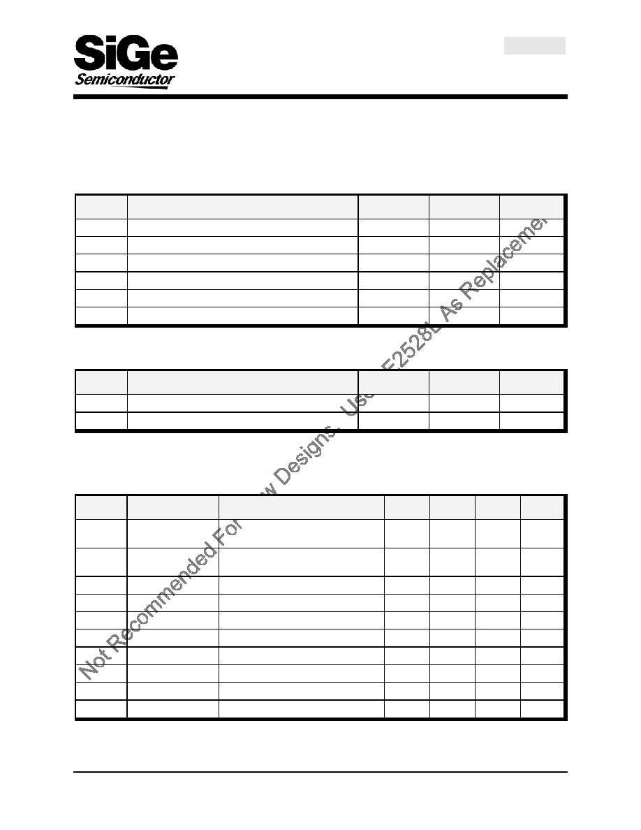 SE2525L RangeCharger™ 2.4GHz Power Amplifier with Power Detector Preliminary Information 28-DST-01 Rev 2.1 Apr-25-2006 Confidential 3 of 12 QA042506 Absolute Maximum Ratings These are stress ratings only. Exposure to stresses beyond these maximum ratings for a long period of time may cause permanent damage to, or affect the reliability of the device. Avoid operating the device outside the recommended operating conditions defined below. This device is ESD sensitive. Handling and assembly of this device should be at ESD protected workstations. Symbol Definition Min. Max. Unit VCC Supply Voltage on pins VCC0, VCC1 VCC2 and VCC3 -0.3 4.0 V VB Bias Control Voltage -0.3 4.0 V VEN Power Amplifier Enable -0.3 4.0 V IN RF Input Power - 4.0 dBm TSTG Storage Temperature Range -40 +150 °C Tj Maximum Junction Temperature - +150 °C Recommended Operating Conditions Symbol Parameter Min. Max. Unit VCC Supply Voltage on pins VCC0, VCC1 VCC2 and VCC3 2.7 3.6 V TA Ambient Temperature -40 85 °C DC Electrical Characteristics Conditions: VCC = VEN = 3.3 V, VB connected to VREG, TA = 25 °C, as measured on SiGe Semiconductor’s SE2525L- EV1 evaluation board, unless otherwise noted. Symbol Parameter Conditions Min. Typ. Max. Unit ICC-802.11b Supply Current POUT = 23 dBm, 11 Mbps CCK signal, BT = 0.45 - 230 - mA ICC-802.11g Supply Current POUT = 19 dBm, 54 Mbps OFDM signal, 64 QAM - 160 - mA ICC-1DB Supply Current POUT = P1dB, No modulation - 340 - mA IOFF Supply Current VEN = 0 V - 10 - µA VREG Regulator Voltage IREG = 120 µA (1) - 2.5 2.75 V IREG Regulator current - - - 500 µA VENH Logic High Voltage TA = -40 to 85 °C, VCC = 2.7 to 3.6 V 1.3 - VCC V VENL Logic Low Voltage TA = -40 to 85 °C, VCC = 2.7 to 3.6 V 0 - 0.5 V VB Bias voltage - 0 - VREG V IB Bias current VB = 2.75 V - - 120 µA (1) No coupling or circuitry that provides a DC path to ground should be connected to the VREG pin. Connection to the VB is allowed. |
|
|
Link URL |
| Does ALLDATASHEET help your business so far? [ DONATE ] |
About Alldatasheet | Advertisement | Contact us | Privacy Policy | Link to Datasheet | Link Exchange | Manufacturer List All Rights Reserved©Alldatasheet.com |
| Russian : Alldatasheetru.com | Korean : Alldatasheet.co.kr | Spanish : Alldatasheet.es | French : Alldatasheet.fr | Italian : Alldatasheetit.com Portuguese : Alldatasheetpt.com | Polish : Alldatasheet.pl | Vietnamese : Alldatasheet.vn Indian : Alldatasheet.in | Mexican : Alldatasheet.com.mx | British : Alldatasheet.co.uk | New Zealand : Alldatasheet.co.nz |
|
Family Site : ic2ic.com |
icmetro.com |
 New Zealand ▼
 English
 Chinese
 German
 Japanese
 Russian
 Korean
 Spanish
 French
 Italian
 Portuguese
 Polish
 Vietnamese
 Indian
 Mexican
 British
 New Zealand