|
Electronic Components Datasheet Search |
|
|
Electronic Components Datasheet Search |
|
ADL8154ACPZN-R7 Datasheet(PDF) 20 Page - Analog Devices |
|
|
|||||||||||||||||||||||||||||
ADL8154ACPZN-R7 Datasheet(HTML) 20 Page - Analog Devices |
|
|
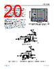
20 / 23 page 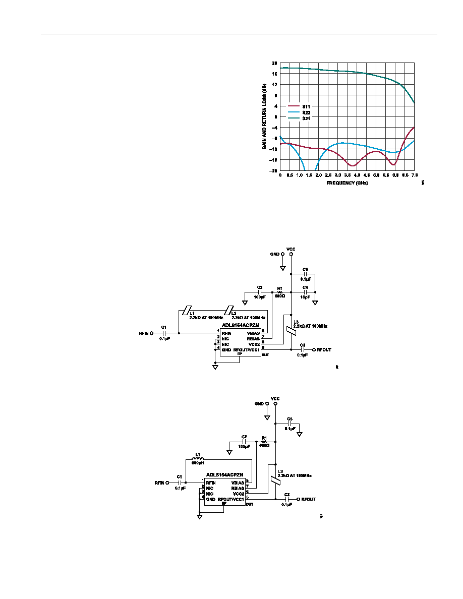 Data Sheet ADL8154 APPLICATIONS INFORMATION analog.com Rev. 0 | 20 of 23 The basic connections for operating the ADL8154 over the speci- fied frequency range are shown in Figure 82, and it also shows the configuration used to characterize and qualify the ADL8154. To set ICQ, connect a resistor (R1) between the RBIAS and VCC1 and VCC2 pins. A default value of 680 Ω is recommended, which results in a nominal ICQ of 125 mA. Table 9 shows how the ICQ and ICQ _AMP varies vs. the RBIAS. The RBIAS pin also draws a current that varies with the value of RBIAS (see Table 9). Do not leave the RBIAS pin open. Figure 83 shows an alternate application circuit for use when there is a requirement to reduce the number of components around the ADL8154 to save space. In this alternate application circuit, the C4 and L2 components are removed, and L1 is changed from a 2.2 kΩ ferrite bead to a 900 nH wire wound inductor (Coilcraft 0402DF-901XJRW). S-parameter performance for the alternate ap- plication circuit is shown in Figure 81. Compare Figure 81 to Figure 9 and Figure 12 to see that there is no performance impact on the S-parameters compared to the nominal performance shown in Figure 9 and Figure 12. Figure 81. Broadband S-Parameters, L2 and C4 Removed, and L1 Changed from 2.2 kΩ Ferrite Bead to 900 nH Wire Wound Inductor Figure 82. Typical Application Circuit Figure 83. Alternate Application Circuit, C4 and L2 Removed and L1 Changed from 2.2 kΩ Ferrite Bead to 900 nH Wire Wound Inductor |
|
|
Link URL |
| Does ALLDATASHEET help your business so far? [ DONATE ] |
About Alldatasheet | Advertisement | Contact us | Privacy Policy | Link to Datasheet | Link Exchange | Manufacturer List All Rights Reserved©Alldatasheet.com |
| Russian : Alldatasheetru.com | Korean : Alldatasheet.co.kr | Spanish : Alldatasheet.es | French : Alldatasheet.fr | Italian : Alldatasheetit.com Portuguese : Alldatasheetpt.com | Polish : Alldatasheet.pl | Vietnamese : Alldatasheet.vn Indian : Alldatasheet.in | Mexican : Alldatasheet.com.mx | British : Alldatasheet.co.uk | New Zealand : Alldatasheet.co.nz |
|
Family Site : ic2ic.com |
icmetro.com |
 New Zealand ▼
 English
 Chinese
 German
 Japanese
 Russian
 Korean
 Spanish
 French
 Italian
 Portuguese
 Polish
 Vietnamese
 Indian
 Mexican
 British
 New Zealand