 |
Electronic Components Datasheet Search |
|
|
Electronic Components Datasheet Search |
|
GS-R51212S Datasheet(PDF) 4 Page - STMicroelectronics |
|
|
|||||||||||||||||||||||||||||
GS-R51212S Datasheet(HTML) 4 Page - STMicroelectronics |
|
|
4 / 8 page 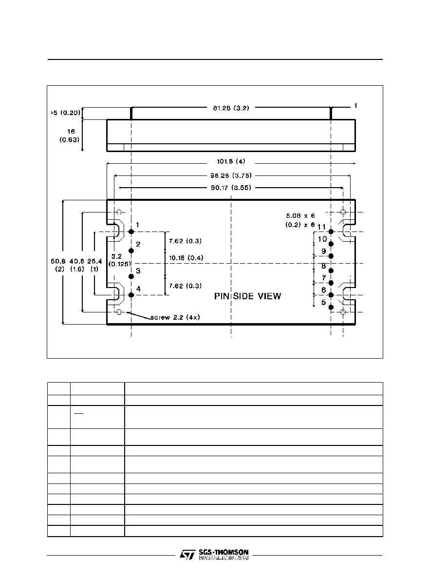 Package R. Dimensions in mm (inches). CONNECTION DIAGRAM AND MECHANICAL DATA 4/8 PIN DESCRIPTION Pin Function Description 1 GND IN Return for input voltage source. Internally connected to pin 7. 2 EN. Inhibit/Enable control input. The converter is ON (ENABLE) when the voltage applied to this pin is lower than 0.8V. The converter is OFF (INHIBIT) when this pin is unconnected or the input voltage is in the range of 1.2 to Vi. 3 P.F. Power Fail programmable input. If unconnected the Power Fail threshold voltage is 11V with 1V hysteresis (factory setting). 4 + Vin DC input voltage. Recommended maximum voltage is 40V. 5RT Reset output (active high). When the supply voltage +Vin and the regulated output voltage +Vo1 are in the correct range this signal is generated after a delay time of 100ms typical. 6 Vo + 5V Regulated +5.1V output voltage. 7 GND 1 Return for output 1 current path. Internally connected to pin 1. 8 Vo + 12/15V Regulated +12 or +15V output. 9 Vo – 12/15V Regulated – 12 or – 15V output. 10 ADJ. External adjustment for output voltages ±12 and ±15V. 11 GND Aux. Return for ±12 and ±15V output current path. GS-R51212S/GS-R51515S |
|
|
Link URL |
| Does ALLDATASHEET help your business so far? [ DONATE ] |
About Alldatasheet | Advertisement | Contact us | Privacy Policy | Link to Datasheet | Link Exchange | Manufacturer List All Rights Reserved©Alldatasheet.com |
| Russian : Alldatasheetru.com | Korean : Alldatasheet.co.kr | Spanish : Alldatasheet.es | French : Alldatasheet.fr | Italian : Alldatasheetit.com Portuguese : Alldatasheetpt.com | Polish : Alldatasheet.pl | Vietnamese : Alldatasheet.vn Indian : Alldatasheet.in | Mexican : Alldatasheet.com.mx | British : Alldatasheet.co.uk | New Zealand : Alldatasheet.co.nz |
|
Family Site : ic2ic.com |
icmetro.com |
 New Zealand ▼
 English
 Chinese
 German
 Japanese
 Russian
 Korean
 Spanish
 French
 Italian
 Portuguese
 Polish
 Vietnamese
 Indian
 Mexican
 British
 New Zealand


