 |
Electronic Components Datasheet Search |
|
|
Electronic Components Datasheet Search |
|
IS25LP02GJ-RHLA3 Datasheet(PDF) 76 Page - Integrated Silicon Solution, Inc |
|
|
|||||||||||||||||||||||||||||
IS25LP02GJ-RHLA3 Datasheet(HTML) 76 Page - Integrated Silicon Solution, Inc |
|
|
76 / 182 page 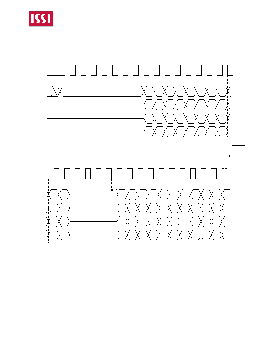 IS25LP02GJ IS25WP02GJ Integrated Silicon Solution, Inc.- www.issi.com 76 Rev.A 10/02/2025 Figure 8.16 Fast Read Quad I/O Sequence (EBh [EXTADD=1] or ECh, 4-byte address) CE # SCK 5 1 Data Out 1 Instruction = EBh/ECh 20 CE # SCK 4 0 28 24 4-byte Address High Impedance 16 12 8 0 1 2 3 4 5 6 7 8 9 10 11 12 13 14 15 16 17 18 19 20 21 22 23 24 25 26 27 28 29 30 31 Mode 3 Mode 0 ... tV IO0 IO1 4 0 5 1 4 0 5 1 4 0 IO0 IO1 21 5 1 29 25 17 13 9 22 6 2 30 26 18 14 10 23 7 3 31 27 19 15 11 IO2 IO3 6 2 6 2 6 2 7 3 7 3 7 3 Data Out 2 Data Out 3 IO2 IO3 1 0 5 1 ... 4 0 ... 2 6 2 ... 3 7 3 ... 5 4 6 7 6 Dummy Cycles Data Out 4 Data Out 5 4 0 5 1 6 2 7 3 Mode Bits Notes: 1. If the mode bits=AXh (where X is don’t care), it can execute the AX read mode (without command). When the mode bits are different from AXh, the device exits the AX read operation. 2. Number of dummy cycles depends on clock speed. Detailed information in Table 6.11 Read Dummy Cycles. 3. Sufficient dummy cycles are required to avoid I/O contention. If the number of dummy cycles and AX bits cycles are same, then X should be Hi-Z. |
|
Link URL |
| Does ALLDATASHEET help your business so far? [ DONATE ] |
About Alldatasheet | Advertisement | Contact us | Privacy Policy | Link to Datasheet | Link Exchange | Manufacturer List All Rights Reserved©Alldatasheet.com |
| Russian : Alldatasheetru.com | Korean : Alldatasheet.co.kr | Spanish : Alldatasheet.es | French : Alldatasheet.fr | Italian : Alldatasheetit.com Portuguese : Alldatasheetpt.com | Polish : Alldatasheet.pl | Vietnamese : Alldatasheet.vn Indian : Alldatasheet.in | Mexican : Alldatasheet.com.mx | British : Alldatasheet.co.uk | New Zealand : Alldatasheet.co.nz |
|
Family Site : ic2ic.com |
icmetro.com |
 New Zealand ▼
 English
 Chinese
 German
 Japanese
 Russian
 Korean
 Spanish
 French
 Italian
 Portuguese
 Polish
 Vietnamese
 Indian
 Mexican
 British
 New Zealand


