 |
Electronic Components Datasheet Search |
|
|
Electronic Components Datasheet Search |
|
ADRF5203BCCZN-R7 Datasheet(PDF) 1 Page - Analog Devices |
|
|
|||||||||||||||||||||||||||||
ADRF5203BCCZN-R7 Datasheet(HTML) 1 Page - Analog Devices |
|
|
1 / 15 page 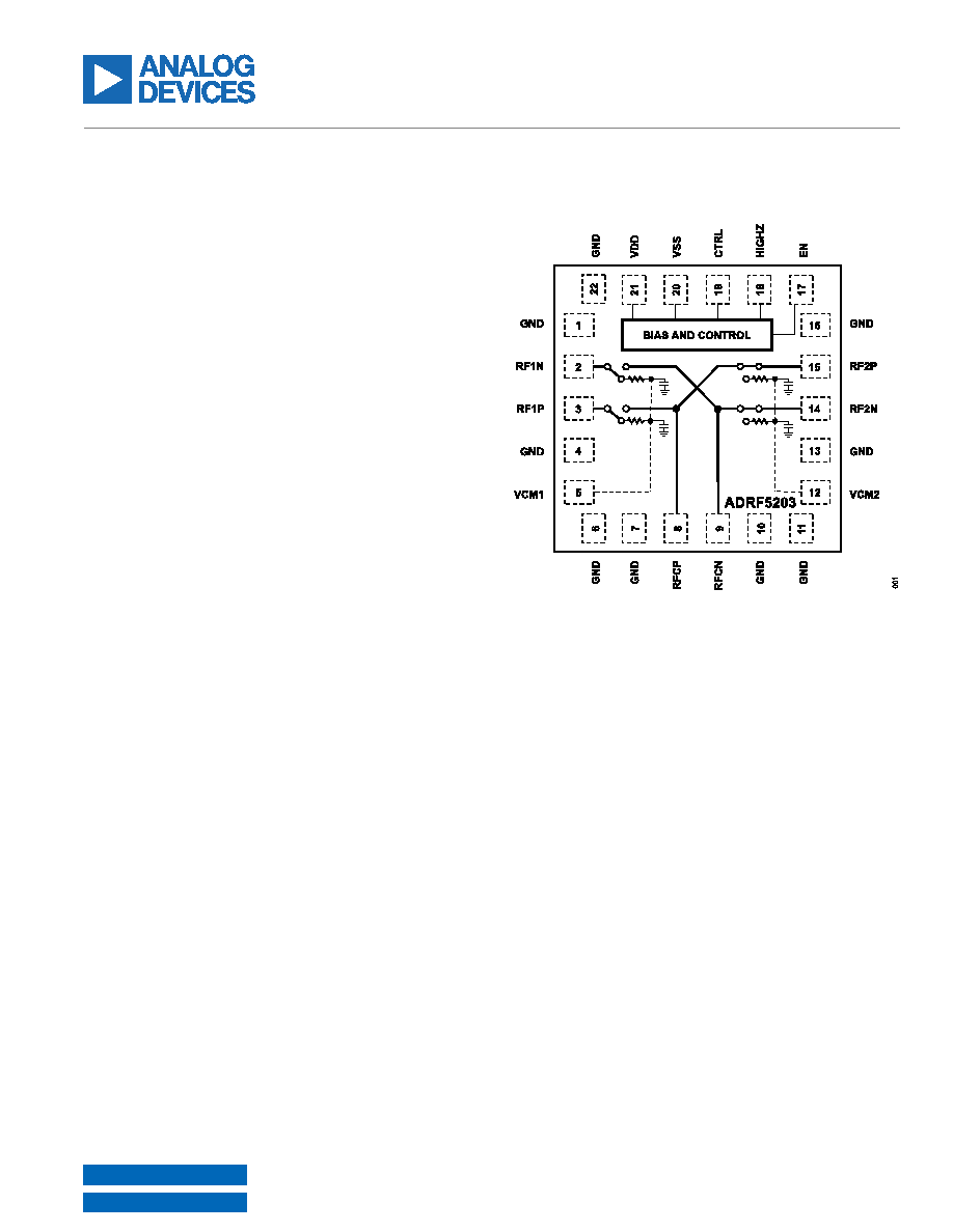 Data Sheet ADRF5203 DC to 12GHz, Differential, Nonreflective, Silicon SPDT Switch Rev. 0 DOCUMENT FEEDBACK TECHNICAL SUPPORT Information furnished by Analog Devices is believed to be accurate and reliable "as is". However, no responsibility is assumed by Analog Devices for its use, nor for any infringements of patents or other rights of third parties that may result from its use. Specifications subject to change without notice. No license is granted by implication or otherwise under any patent or patent rights of Analog Devices. Trademarks and registered trademarks are the property of their respective owners. All Analog Devices products contained herein are subject to release and availability. FEATURES ► Frequency range: DC to 12GHz ► DC voltage range: ±8V ► DC RON: <2.5Ω ► Fully differential 100Ω design ► Low insertion loss ► 0.65dB typical to 6GHz ► 0.9dB typical to 10GHz ► 1.1dB typical to 12GHz ► High isolation (terminated mode) ► >48 dB typical to 6GHz ► >41 dB typical to 10GHz ► >37 dB typical to 12GHz ► High input linearity ► P0.1dB: 33dBm typical ► IP3: 51dBm typical ► High power handling ► 31dBm through path ► 24dBm terminated path ► On time: 1.9µs ► 0.1dB settling time: 3.2µs ► All off state control ► Termination control: 100Ω differential or high-Z (reflective) ► 22-terminal, 3mm × 3mm, RoHS-compliant, land grid array (LGA) package APPLICATIONS ► Test instrumentation ► Data converter interfaces ► High data rate interfaces FUNCTIONAL BLOCK DIAGRAM Figure 1. Functional Block Diagram GENERAL DESCRIPTION The ADRF5203 is a silicon, differential, SPDT switch. The ADRF5203 operates from DC to 12GHz with an insertion loss of better than 1.1dB and an isolation higher than 37dB. The device has a DC input voltage range of ±8 V and RF input power handling of differential 31dBm for through paths and 24dBm for terminated paths. The ADRF5203 operates with dual-supply voltages of ±12V. The ADRF5203 employs complementary metal-oxide semiconductor (CMOS)- and low voltage transistor logic (LVTTL)-compatible con- trols. The ADRF5203 has an enable control to feature its all off state function. The high-Z control selects the termination (100Ω or high-Z) on the unselected RF channel. The ADRF5203 comes in a 22-terminal, 3mm × 3mm, RoHS com- pliant, land grid array (LGA) package and can operate from −40°C to +105°C. |
Similar Part No. - ADRF5203BCCZN-R7 |
|
Similar Description - ADRF5203BCCZN-R7 |
|
|
|
Link URL |
| Does ALLDATASHEET help your business so far? [ DONATE ] |
About Alldatasheet | Advertisement | Contact us | Privacy Policy | Link to Datasheet | Link Exchange | Manufacturer List All Rights Reserved©Alldatasheet.com |
| Russian : Alldatasheetru.com | Korean : Alldatasheet.co.kr | Spanish : Alldatasheet.es | French : Alldatasheet.fr | Italian : Alldatasheetit.com Portuguese : Alldatasheetpt.com | Polish : Alldatasheet.pl | Vietnamese : Alldatasheet.vn Indian : Alldatasheet.in | Mexican : Alldatasheet.com.mx | British : Alldatasheet.co.uk | New Zealand : Alldatasheet.co.nz |
|
Family Site : ic2ic.com |
icmetro.com |
 New Zealand ▼
 English
 Chinese
 German
 Japanese
 Russian
 Korean
 Spanish
 French
 Italian
 Portuguese
 Polish
 Vietnamese
 Indian
 Mexican
 British
 New Zealand


