|
Electronic Components Datasheet Search |
|
|
Electronic Components Datasheet Search |
|
M95512-R Datasheet(PDF) 23 Page - STMicroelectronics |
|
|
|||||||||||||||||||||||||||||
M95512-R Datasheet(HTML) 23 Page - STMicroelectronics |
|
|
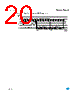
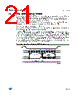
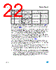
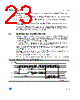
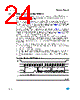
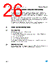
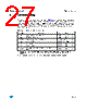
23 / 39 page 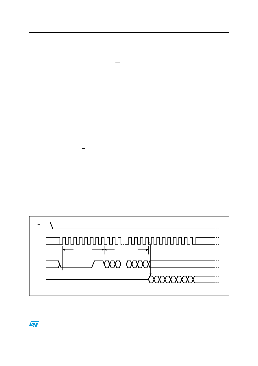 M95512-W, M95512-R Instructions 23/39 Regardless of the order of the two events, the Hardware Protected Mode (HPM) can be entered: ● by setting the Status Register Write Disable (SRWD) bit after driving Write Protect (W) Low ● or by driving Write Protect (W) Low after setting the Status Register Write Disable (SRWD) bit. The only way to exit the Hardware Protected Mode (HPM) once entered is to pull Write Protect (W) High. If Write Protect (W) is permanently tied High, the Hardware Protected Mode (HPM) can never be activated, and only the Software Protected Mode (SPM), using the Block Protect (BP1, BP0) bits of the Status Register, can be used. 6.5 Read from Memory Array (READ) As shown in Figure 11, to send this instruction to the device, Chip Select (S) is first driven Low. The bits of the instruction byte and address bytes are then shifted in, on Serial Data Input (D). The address is loaded into an internal address register, and the byte of data at that address is shifted out, on Serial Data Output (Q). If Chip Select (S) continues to be driven Low, the internal address register is automatically incremented, and the byte of data at the new address is shifted out. When the highest address is reached, the address counter rolls over to zero, allowing the Read cycle to be continued indefinitely. The whole memory can, therefore, be read with a single READ instruction. The Read cycle is terminated by driving Chip Select (S) High. The rising edge of the Chip Select (S) signal can occur at any time during the cycle. The first byte addressed can be any byte within any page. The instruction is not accepted, and is not executed, if a Write cycle is currently in progress. Figure 11. Read from Memory Array (READ) sequence C D AI01793D S Q 15 2 1 3456789 10 20 21 22 23 24 25 26 27 14 13 3210 28 29 30 76543 1 7 0 High Impedance Data Out 1 Instruction 16-Bit Address 0 MSB MSB 2 31 Data Out 2 |
|
Link URL |
| Does ALLDATASHEET help your business so far? [ DONATE ] |
About Alldatasheet | Advertisement | Contact us | Privacy Policy | Link to Datasheet | Link Exchange | Manufacturer List All Rights Reserved©Alldatasheet.com |
| Russian : Alldatasheetru.com | Korean : Alldatasheet.co.kr | Spanish : Alldatasheet.es | French : Alldatasheet.fr | Italian : Alldatasheetit.com Portuguese : Alldatasheetpt.com | Polish : Alldatasheet.pl | Vietnamese : Alldatasheet.vn Indian : Alldatasheet.in | Mexican : Alldatasheet.com.mx | British : Alldatasheet.co.uk | New Zealand : Alldatasheet.co.nz |
|
Family Site : ic2ic.com |
icmetro.com |
 New Zealand ▼
 English
 Chinese
 German
 Japanese
 Russian
 Korean
 Spanish
 French
 Italian
 Portuguese
 Polish
 Vietnamese
 Indian
 Mexican
 British
 New Zealand