|
Electronic Components Datasheet Search |
|
|
Electronic Components Datasheet Search |
|
ADG774ABCPZ-R2 Datasheet(PDF) 7 Page - Analog Devices |
|
|
|||||||||||||||||||||||||||||
ADG774ABCPZ-R2 Datasheet(HTML) 7 Page - Analog Devices |
|
|
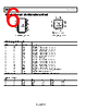
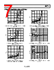
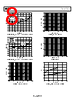
7 / 14 page 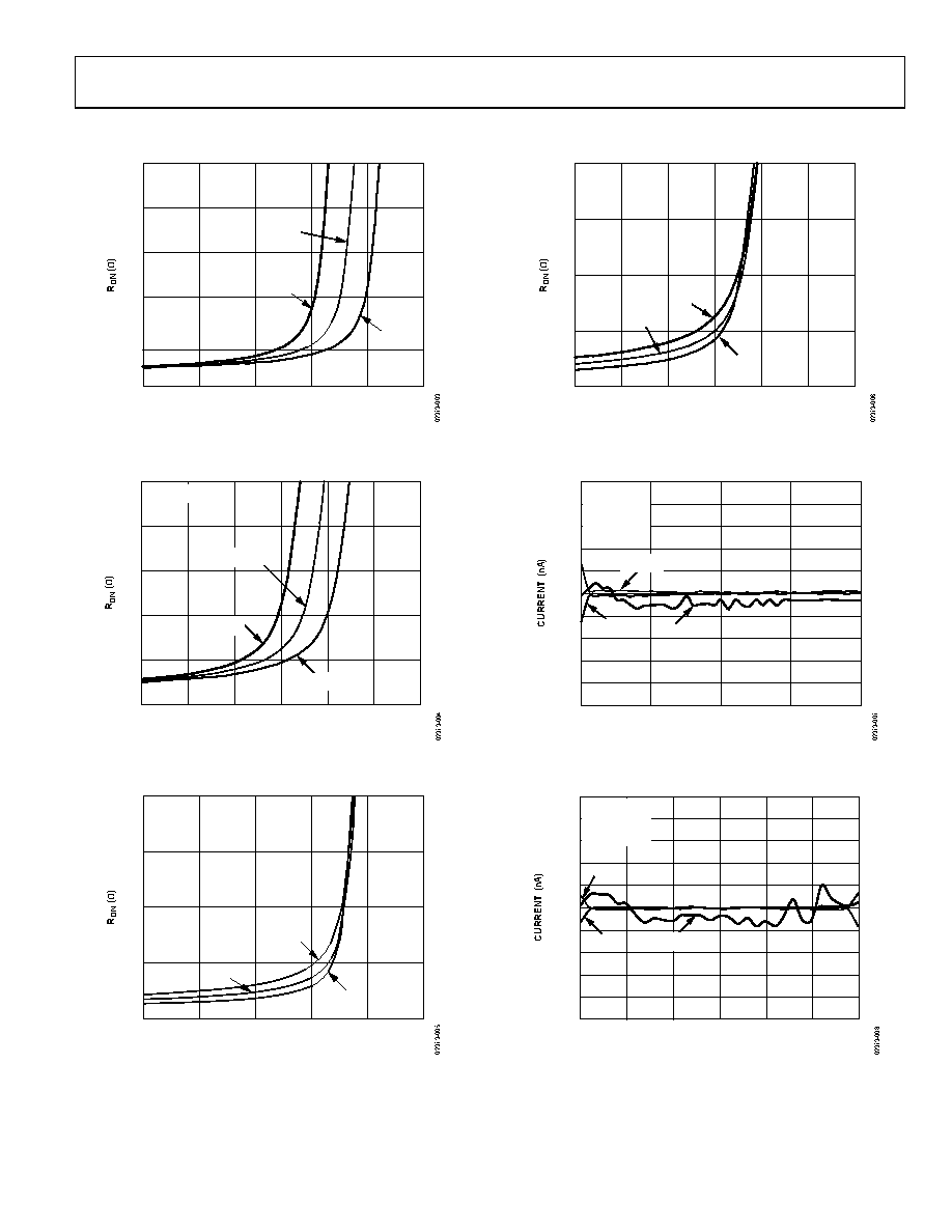 Data Sheet ADG774A Rev. C | Page 7 of 14 TYPICAL PERFORMANCE CHARACTERISTICS 20 0 05 VS/VD (V) 16 12 8 4 1 234 VDD = 5.0V VDD = 4.5V VDD = 5.5V TA = 25°C Figure 4. On Resistance as a Function of Drain (VD) or Source (VS) Voltage for VDD = 5 V ± 10% 20 0 03.0 VS/VD (V) 16 12 8 4 0.5 1.0 1.5 2.0 2.5 VDD = 3.0V TA = 25°C VDD = 2.7V VDD = 3.3V Figure 5. On Resistance as a Function of Drain (VD) or Source (VS) Voltage for VDD = 3 V ± 10% 20 0 05 VS/VD (V) 15 10 5 1 234 VDD = 5V +85°C –40°C +25°C Figure 6. On Resistance as a Function of Drain (VD) or Source (VS) Voltage for Different Temperatures with 5 V Single Supplies 20 0 03.0 VS/VD (V) 15 10 5 0.5 1.0 1.5 2.0 2.5 VDD = 3V +85°C –40°C +25°C Figure 7. On Resistance as a Function of Drain (VD) or Source (VS) Voltage for Different Temperatures with 3 V Single Supplies 0.025 –0.025 04 VS/VD (V) 0.020 0.015 0.010 0.005 0 –0.005 –0.010 –0.015 –0.020 123 VS IS (OFF) IS, ID (ON) VDD = 5.0V VSS = 0V TEMP = 25°C VD = VDD – VS ID (OFF) Figure 8. Leakage Current as a Function of Drain (VD) or Source (VS) Voltage for VDD = 5 V 0.025 –0.025 03.0 VS/VD (V) VS 0.020 0.015 0.010 0.005 0 –0.005 –0.010 –0.015 –0.020 0.5 1.0 1.5 2.0 2.5 IS (OFF) VDD = 3.0V VSS = 0V TEMP = 25°C VD = VDD – VS ID (OFF) IS, ID (ON) Figure 9. Leakage Current as a Function of Drain (VD) or Source (VS) Voltage for VDD = 3 V |
|
|
Link URL |
| Does ALLDATASHEET help your business so far? [ DONATE ] |
About Alldatasheet | Advertisement | Contact us | Privacy Policy | Link to Datasheet | Link Exchange | Manufacturer List All Rights Reserved©Alldatasheet.com |
| Russian : Alldatasheetru.com | Korean : Alldatasheet.co.kr | Spanish : Alldatasheet.es | French : Alldatasheet.fr | Italian : Alldatasheetit.com Portuguese : Alldatasheetpt.com | Polish : Alldatasheet.pl | Vietnamese : Alldatasheet.vn Indian : Alldatasheet.in | Mexican : Alldatasheet.com.mx | British : Alldatasheet.co.uk | New Zealand : Alldatasheet.co.nz |
|
Family Site : ic2ic.com |
icmetro.com |
 New Zealand ▼
 English
 Chinese
 German
 Japanese
 Russian
 Korean
 Spanish
 French
 Italian
 Portuguese
 Polish
 Vietnamese
 Indian
 Mexican
 British
 New Zealand