|
Electronic Components Datasheet Search |
|
|
Electronic Components Datasheet Search |
|
AD8422ARMZ-R7 Datasheet(PDF) 23 Page - Analog Devices |
|
|
|||||||||||||||||||||||||||||
AD8422ARMZ-R7 Datasheet(HTML) 23 Page - Analog Devices |
|
|
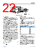
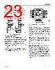
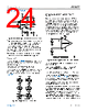
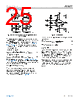
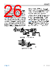
23 / 28 page 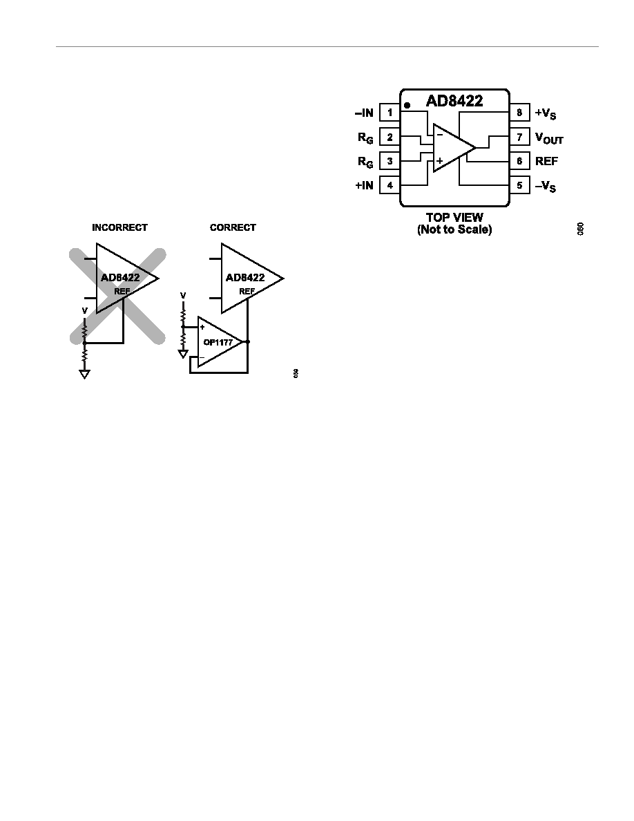 Data Sheet AD8422 THEORY OF OPERATION analog.com Rev. C | 23 of 28 For best performance, maintain a source impedance to the REF terminal that is below 1 Ω. As shown in Figure 56, the reference terminal, REF, is at one end of a 10 kΩ resistor. Additional impe- dance at the REF terminal adds to this 10 kΩ resistor and results in amplification of the signal connected to the positive input. The amplification from the additional RREF can be calculated as 2(10 kΩ + RREF)/(20 kΩ + RREF) Only the positive signal path is amplified; the negative path is unaffected. This uneven amplification degrades CMRR. Figure 57. Driving the Reference Pin (REF) INPUT VOLTAGE RANGE The 3-op-amp architecture of the AD8422 applies gain in the first stage before removing common-mode voltage with the difference amplifier stage. Internal nodes between the first and second stages (Node 1 and Node 2 in Figure 56) experience a combination of a gained signal, a common-mode signal, and a diode drop. The voltage supplies can limit the combined signal, even when the individual input and output signals are not limited. Figure 11 through Figure 14 show this limitation in detail. LAYOUT To ensure optimum performance of the AD8422 at the PCB level, take care in the design of the board layout. To aid in this task, the pins of the AD8422 are arranged in a logical manner. Figure 58. Pinout Diagram Common-Mode Rejection Ratio over Frequency Poor layout can cause some of the common-mode signals to be converted to differential signals before reaching the in-amp. Such conversions occur when one input path has a frequency response that is different from the other. To maintain high CMRR over fre- quency, closely match the input source impedance and capacitance of each path. Place additional source resistance in the input path (for example, for input protection) close to the in-amp inputs, which minimizes their interaction with parasitic capacitance from the PCB traces. Parasitic capacitance at the gain setting pins (RG) can also affect CMRR over frequency. If the board design has a component at the gain setting pins (for example, a switch or jumper), choose a component such that the parasitic capacitance is as small as possible. Power Supplies and Grounding Use a stable dc voltage to power the instrumentation amplifier. Noise on the supply pins can adversely affect performance. Place a 0.1 µF capacitor as close as possible to each supply pin. Because the length of the bypass capacitor leads is critical at high frequency, surface-mount capacitors are recommended. A parasitic inductance in the bypass ground trace works against the low impedance created by the bypass capacitor. As shown in Figure 59, a 10 µF capacitor can be used farther away from the device. For larger value capacitors, intended to be effective at lower frequencies, the current return path distance is less critical. In most cases, this capacitor can be shared by other local precision integrated circuits. |
|
Link URL |
| Does ALLDATASHEET help your business so far? [ DONATE ] |
About Alldatasheet | Advertisement | Contact us | Privacy Policy | Link to Datasheet | Link Exchange | Manufacturer List All Rights Reserved©Alldatasheet.com |
| Russian : Alldatasheetru.com | Korean : Alldatasheet.co.kr | Spanish : Alldatasheet.es | French : Alldatasheet.fr | Italian : Alldatasheetit.com Portuguese : Alldatasheetpt.com | Polish : Alldatasheet.pl | Vietnamese : Alldatasheet.vn Indian : Alldatasheet.in | Mexican : Alldatasheet.com.mx | British : Alldatasheet.co.uk | New Zealand : Alldatasheet.co.nz |
|
Family Site : ic2ic.com |
icmetro.com |
 New Zealand ▼
 English
 Chinese
 German
 Japanese
 Russian
 Korean
 Spanish
 French
 Italian
 Portuguese
 Polish
 Vietnamese
 Indian
 Mexican
 British
 New Zealand