|
Electronic Components Datasheet Search |
|
|
Electronic Components Datasheet Search |
|
ST5088FN Datasheet(PDF) 9 Page - STMicroelectronics |
|
|
|||||||||||||||||||||||||||||
ST5088FN Datasheet(HTML) 9 Page - STMicroelectronics |
|
|
9 / 33 page 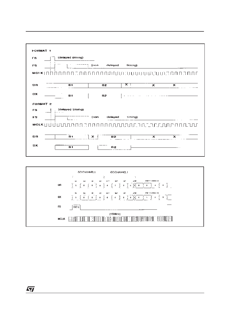 output shifts data out from the voice data register on the rising edges of MCLK. Serial voice data is shifted into DR input during the same time slot on the falling edges of MCLK. DX is in the high impedance Tristate condition when in the non selected time slots. Control Interface: Control information or data is written into or read- back from PIAFE via the serial control port con- sisting of control clock CCLK, serial data input CI and output CO, and Chip Select input, CS-. All control instructions require 2 bytes as listed in Ta- ble 1, with the exception of a single byte power- up/down command. To shift control data into ST5088, CCLK must be pulsed high 8 times while CS- is low. Data on CI input is shifted into the serial input register on the rising edge of each CCLK pulse. After all data is shifted in, the content of the input shift register is decoded, and may indicate that a 2nd byte of control data will follow. This second byte may either be defined by a second byte-wide CS- pulse or may follow the first contiguously, i.e. it is not mandatory for CS- to return high in between the first and second control bytes. At the end of Figure 2: GCI Interface Frame Structure Figure 1: Digital Interface Format ST5088 9/33 |
|
Link URL |
| Does ALLDATASHEET help your business so far? [ DONATE ] |
About Alldatasheet | Advertisement | Contact us | Privacy Policy | Link to Datasheet | Link Exchange | Manufacturer List All Rights Reserved©Alldatasheet.com |
| Russian : Alldatasheetru.com | Korean : Alldatasheet.co.kr | Spanish : Alldatasheet.es | French : Alldatasheet.fr | Italian : Alldatasheetit.com Portuguese : Alldatasheetpt.com | Polish : Alldatasheet.pl | Vietnamese : Alldatasheet.vn Indian : Alldatasheet.in | Mexican : Alldatasheet.com.mx | British : Alldatasheet.co.uk | New Zealand : Alldatasheet.co.nz |
|
Family Site : ic2ic.com |
icmetro.com |
 New Zealand ▼
 English
 Chinese
 German
 Japanese
 Russian
 Korean
 Spanish
 French
 Italian
 Portuguese
 Polish
 Vietnamese
 Indian
 Mexican
 British
 New Zealand