|
Electronic Components Datasheet Search |
|
|
Electronic Components Datasheet Search |
|
AD5667RBCPZ-R2 Datasheet(PDF) 23 Page - Analog Devices |
|
|
|||||||||||||||||||||||||||||
AD5667RBCPZ-R2 Datasheet(HTML) 23 Page - Analog Devices |
|
|
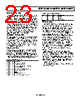
23 / 32 page  AD5627R/AD5647R/AD5667R, AD5627/AD5667 Rev. 0 | Page 23 of 32 INPUT SHIFT REGISTER The input shift register is 24 bits wide. Data is loaded into the device as a 24-bit word under the control of a serial clock input, SCL. The timing diagram for this operation is shown in Figure 3. The 8 MSBs make up the command byte. DB23 is reserved and should always be set to 0 when writing to the device. DB22 (S) is used to select multiple byte operation The next three bits are the command bits (C2, C1, C0) that control the mode of operation of the device. See Table 8 for details. The last 3 bits of first byte are the address bits (A2, A1, A0). See Table 9 for details. The rest of the bits are the 16-, 14-, 12-bit data word. The data word comprises the 16-, 14-, 12-bit input code followed by two or four don’t cares for the AD5647R and the AD5627R/AD5627, respectively (see Figure 59 through Figure 61). MULTIPLE BYTE OPERATION Multiple byte operation is supported on the AD56x7R/AD56x7. A 2-byte operation is useful for applications that require fast DAC updating and do not need to change the command byte. The S bit (DB22) in the command register can be set to 1 for 2- byte mode of operation (see Figure 57). For standard 3-byte and 4-byte operation, the S bit (DB22) in the command byte should be set to 0 (see Figure 58). BROADCAST MODE Broadcast addressing is supported on the AD56x7R/AD56x7. Broadcast addressing can be used to synchronously update or power down multiple AD56x7R/AD56x7 devices. Using the broadcast address, the AD56x7R/AD56x7 responds regardless of the states of the address pins. Broadcast is supported only in write mode. The AD56x7R/AD56x7 broadcast address is 00010000. Table 8. Command Definition C2 C1 C0 Command 0 0 0 Write to input register n 0 0 1 Update DAC register n 0 1 0 Write to input register n, update all (software LDAC) 0 1 1 Write to and update DAC channel n 1 0 0 Power up/power down 1 0 1 Reset 1 1 0 LDAC register setup 1 1 1 Internal reference setup (on/off ) Table 9. DAC Address Command A2 A1 A0 ADDRESS (n) 0 0 0 DAC A 0 0 1 DAC B 1 1 1 Both DACs LDAC FUNCTION The AD56x7R/AD56x7 DACs have double-buffered interfaces consisting of two banks of registers, input registers and DAC registers. The input registers are connected directly to the input shift register, and the digital code is transferred to the relevant input register on completion of a valid write sequence. The DAC registers contain the digital codes used by the resistor strings. Access to the DAC registers is controlled by the LDAC pin. When the LDAC pin is high, the DAC registers are latched and the input registers can change state without affecting the contents of the DAC registers. When LDAC is brought low, however, the DAC registers become transparent and the contents of the input registers are transferred to them. The double- buffered interface is useful if the user requires simultaneous updating of all DAC outputs. The user can write to one of the input registers individually and then, by bringing LDAC low when writing to the other DAC input register, all outputs update simultaneously. These parts each contain an extra feature whereby a DAC register is not updated unless its input register has been updated since the last time LDAC was brought low. Normally, when LDAC is brought low, the DAC registers are filled with the contents of the input registers. In the case of the AD56x7R/AD56x7, the DAC register updates only if the input register has changed since the last time the DAC register was updated, thereby removing unnecessary digital crosstalk. The outputs of all DACs can be simultaneously updated, using the hardware LDAC pin. |
|
Link URL |
| Does ALLDATASHEET help your business so far? [ DONATE ] |
About Alldatasheet | Advertisement | Contact us | Privacy Policy | Link to Datasheet | Link Exchange | Manufacturer List All Rights Reserved©Alldatasheet.com |
| Russian : Alldatasheetru.com | Korean : Alldatasheet.co.kr | Spanish : Alldatasheet.es | French : Alldatasheet.fr | Italian : Alldatasheetit.com Portuguese : Alldatasheetpt.com | Polish : Alldatasheet.pl | Vietnamese : Alldatasheet.vn Indian : Alldatasheet.in | Mexican : Alldatasheet.com.mx | British : Alldatasheet.co.uk | New Zealand : Alldatasheet.co.nz |
|
Family Site : ic2ic.com |
icmetro.com |
 New Zealand ▼
 English
 Chinese
 German
 Japanese
 Russian
 Korean
 Spanish
 French
 Italian
 Portuguese
 Polish
 Vietnamese
 Indian
 Mexican
 British
 New Zealand