 |
Electronic Components Datasheet Search |
|
|
Electronic Components Datasheet Search |
|
ST7263BEx Datasheet(PDF) 53 Page - STMicroelectronics |
|
|
|||||||||||||||||||||||||||||
ST7263BEx Datasheet(HTML) 53 Page - STMicroelectronics |
|
|
53 / 186 page 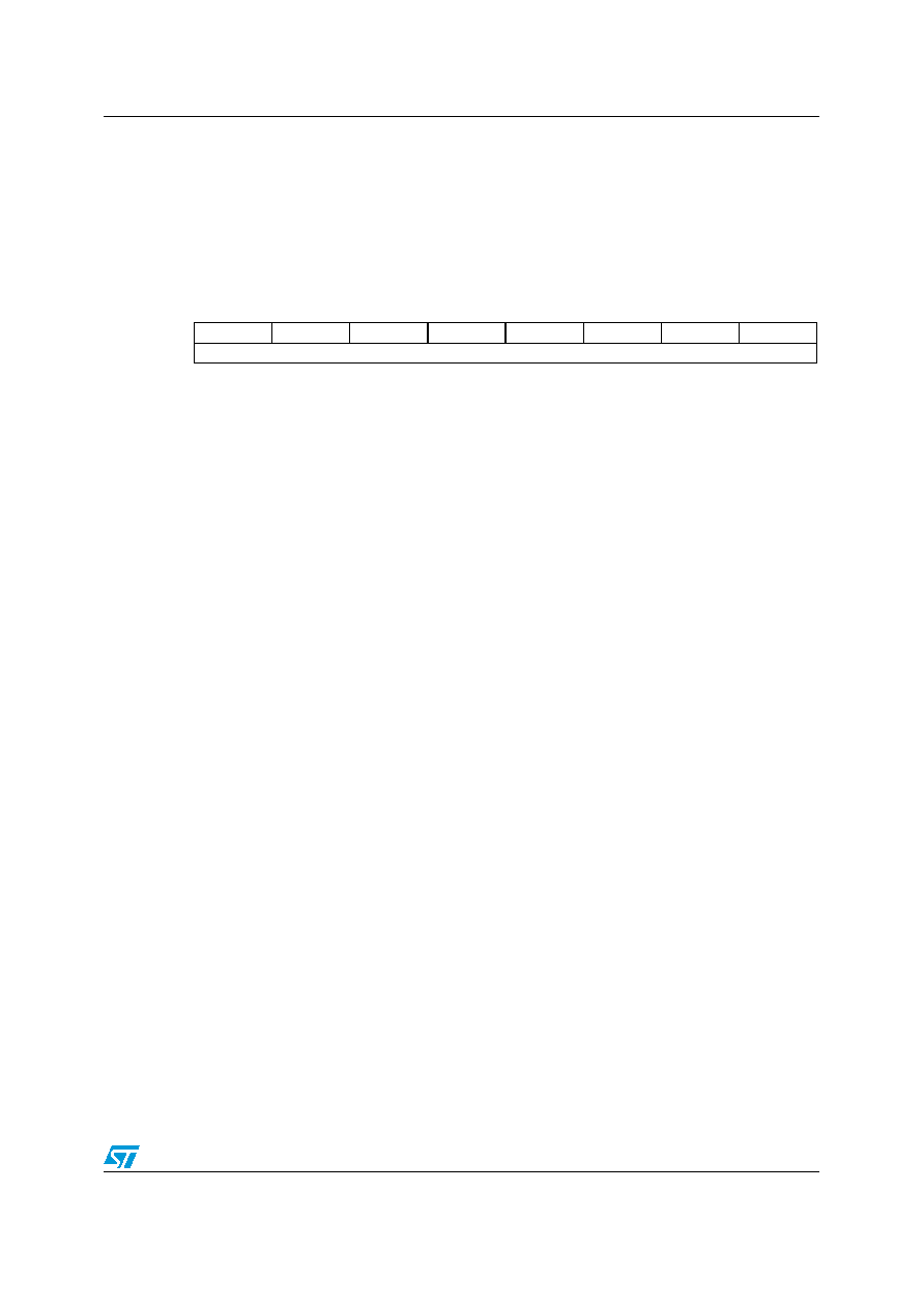 ST7263Bxx Miscellaneous register Doc ID 7516 Rev 8 53/186 10 Miscellaneous register Miscellaneous register (MISCR) Address: 0009h Reset value: 0000 0000 (00h) 7 0 -- -- - SMS USBOE MCO Read/write [7:3] Reserved 2 SMS Slow mode Select. This bit is set by software and only cleared by hardware after a reset. If this bit is set, it enables the use of an internal divide-by-2 clock divider (refer to Figure 18 on page 36). The SMS bit has no effect on the USB frequency. 0: Divide-by-2 disabled and CPU clock frequency is standard 1: Divide-by-2 enabled and CPU clock frequency is halved. 1 USBOE USB enable. If this bit is set, the port PC2 (PB1 on SO24) outputs the USB output enable signal (at “1” when the ST7 USB is transmitting data). Unused bits 7-4 are set. 0 MCO Main Clock Out selection This bit enables the MCO alternate function on the PA0 I/O port. It is set and cleared by software. 0: MCO alternate function disabled (I/O pin free for general-purpose I/O) 1: MCO alternate function enabled (fCPU on I/O port) |
|
Link URL |
| Does ALLDATASHEET help your business so far? [ DONATE ] |
About Alldatasheet | Advertisement | Contact us | Privacy Policy | Link to Datasheet | Link Exchange | Manufacturer List All Rights Reserved©Alldatasheet.com |
| Russian : Alldatasheetru.com | Korean : Alldatasheet.co.kr | Spanish : Alldatasheet.es | French : Alldatasheet.fr | Italian : Alldatasheetit.com Portuguese : Alldatasheetpt.com | Polish : Alldatasheet.pl | Vietnamese : Alldatasheet.vn Indian : Alldatasheet.in | Mexican : Alldatasheet.com.mx | British : Alldatasheet.co.uk | New Zealand : Alldatasheet.co.nz |
|
Family Site : ic2ic.com |
icmetro.com |
 New Zealand ▼
 English
 Chinese
 German
 Japanese
 Russian
 Korean
 Spanish
 French
 Italian
 Portuguese
 Polish
 Vietnamese
 Indian
 Mexican
 British
 New Zealand


