 |
Electronic Components Datasheet Search |
|
|
Electronic Components Datasheet Search |
|
STM8L151C4 Datasheet(PDF) 76 Page - STMicroelectronics |
|
|
|||||||||||||||||||||||||||||
STM8L151C4 Datasheet(HTML) 76 Page - STMicroelectronics |
|
|
76 / 101 page 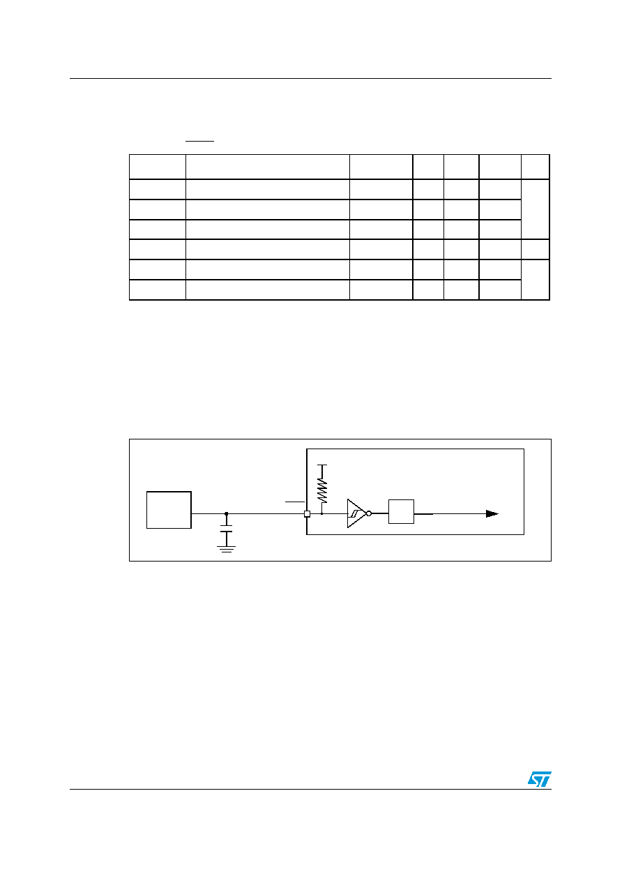 Electrical parameters STM8L151xx, STM8L152xx 76/101 Doc ID 15962 Rev 2 NRST pin Subject to general operating conditions for VDD and TA unless otherwise specified. The reset network shown in Figure 14 protects the device against parasitic resets. The user must ensure that the level on the NRST pin can go below the VIL max. level specified in Table 36. Otherwise the reset is not taken into account internally. Figure 14. Recommended NRST pin configuration Table 36. NRST pin characteristics Symbol Parameter Conditions Min Typ (1) Max Unit VIL(NRST) NRST Input low level voltage (1) 1. Data based on characterization results, not tested in production. VSS 0.8 V VIH(NRST) NRST Input high level voltage (1) 1.4 VDD VOL(NRST) NRST Output low level voltage IOL = 2 mA VDD-0.8 RPU(NRST) NRST Pull-up equivalent resistor (2) 2. The RPU pull-up equivalent resistor is based on a resistive transistor 30 45 60 k Ω VF(NRST) NRST Input filtered pulse (3) 3. Data guaranteed by design, not tested in production. 50 ns VNF(NRST) NRST Input not filtered pulse (3) 300 0.01 μF EXTERNAL RESET CIRCUIT STM8L Filter RPU VDD INTERNAL RESET RSTIN |
|
Link URL |
| Does ALLDATASHEET help your business so far? [ DONATE ] |
About Alldatasheet | Advertisement | Contact us | Privacy Policy | Link to Datasheet | Link Exchange | Manufacturer List All Rights Reserved©Alldatasheet.com |
| Russian : Alldatasheetru.com | Korean : Alldatasheet.co.kr | Spanish : Alldatasheet.es | French : Alldatasheet.fr | Italian : Alldatasheetit.com Portuguese : Alldatasheetpt.com | Polish : Alldatasheet.pl | Vietnamese : Alldatasheet.vn Indian : Alldatasheet.in | Mexican : Alldatasheet.com.mx | British : Alldatasheet.co.uk | New Zealand : Alldatasheet.co.nz |
|
Family Site : ic2ic.com |
icmetro.com |
 New Zealand ▼
 English
 Chinese
 German
 Japanese
 Russian
 Korean
 Spanish
 French
 Italian
 Portuguese
 Polish
 Vietnamese
 Indian
 Mexican
 British
 New Zealand


