 |
Electronic Components Datasheet Search |
|
|
Electronic Components Datasheet Search |
|
STM32F107VB Datasheet(PDF) 58 Page - STMicroelectronics |
|
|
|||||||||||||||||||||||||||||
STM32F107VB Datasheet(HTML) 58 Page - STMicroelectronics |
|
|
58 / 95 page 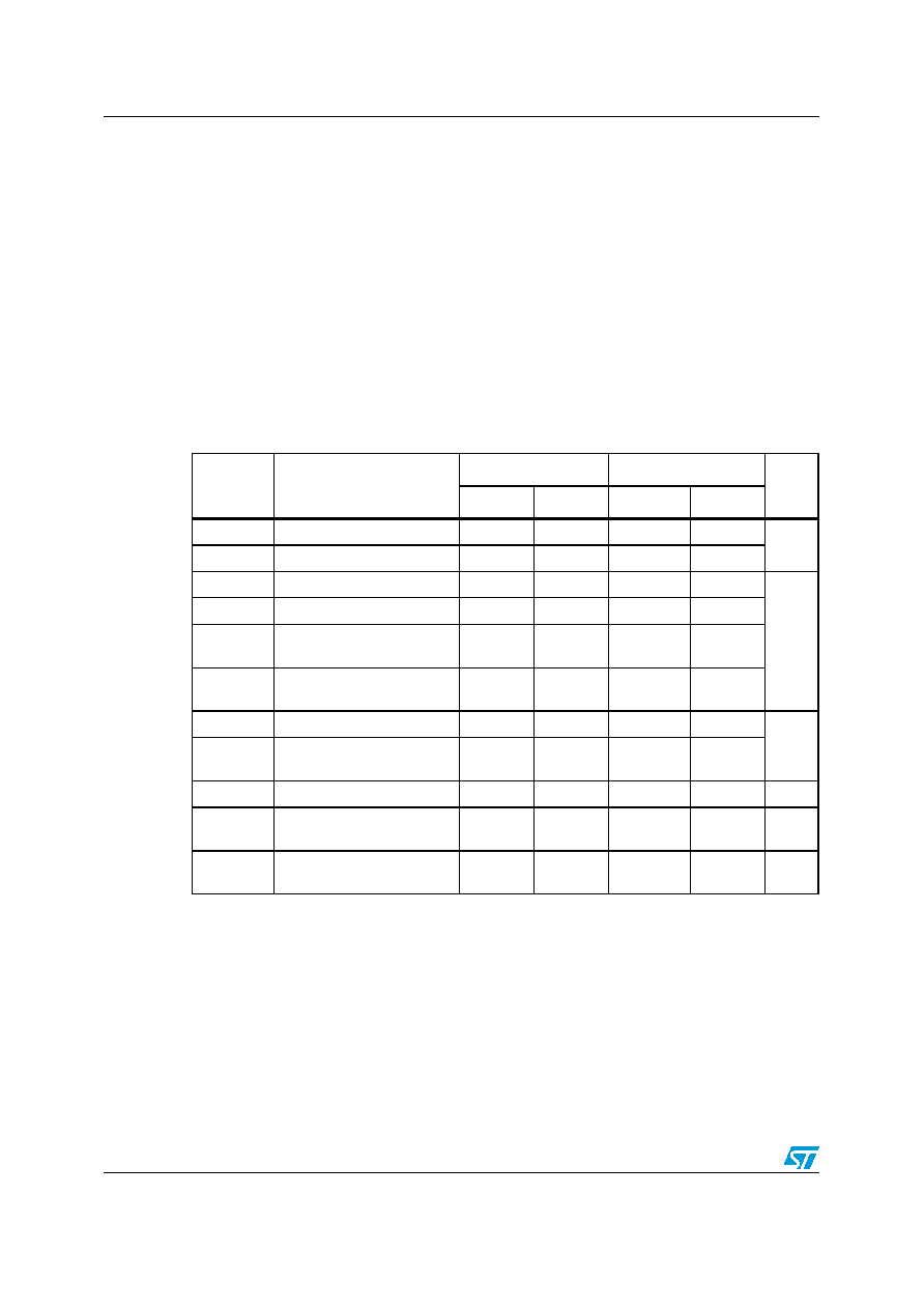 Electrical characteristics STM32F105xx, STM32F107xx 58/95 Doc ID 15274 Rev 4 5.3.15 Communications interfaces I 2C interface characteristics Unless otherwise specified, the parameters given in Table 40 are derived from tests performed under the ambient temperature, fPCLK1 frequency and VDD supply voltage conditions summarized in Table 9. The STM32F105xx and STM32F107xx I 2C interface meets the requirements of the standard I 2C communication protocol with the following restrictions: the I/O pins SDA and SCL are mapped to are not “true” open-drain. When configured as open-drain, the PMOS connected between the I/O pin and VDD is disabled, but is still present. The I 2C characteristics are described in Table 40. Refer also to Section 5.3.12: I/O port characteristics for more details on the input/output alternate function characteristics (SDA and SCL). Table 40. I2C characteristics Symbol Parameter Standard mode I2C(1) 1. Guaranteed by design, not tested in production. Fast mode I2C(1)(2) 2. fPCLK1 must be higher than 2 MHz to achieve the maximum standard mode I 2C frequency. It must be higher than 4 MHz to achieve the maximum fast mode I2C frequency. Unit Min Max Min Max tw(SCLL) SCL clock low time 4.7 1.3 µs tw(SCLH) SCL clock high time 4.0 0.6 tsu(SDA) SDA setup time 250 100 ns th(SDA) SDA data hold time 0(3) 3. The maximum hold time of the Start condition has only to be met if the interface does not stretch the low period of SCL signal. 0(4) 4. The device must internally provide a hold time of at least 300ns for the SDA signal in order to bridge the undefined region of the falling edge of SCL. 900(3) tr(SDA) tr(SCL) SDA and SCL rise time 1000 20 + 0.1Cb 300 tf(SDA) tf(SCL) SDA and SCL fall time 300 300 th(STA) Start condition hold time 4.0 0.6 µs tsu(STA) Repeated Start condition setup time 4.7 0.6 tsu(STO) Stop condition setup time 4.0 0.6 os tw(STO:STA) Stop to Start condition time (bus free) 4.7 1.3 os Cb Capacitive load for each bus line 400 400 pF |
|
Link URL |
| Does ALLDATASHEET help your business so far? [ DONATE ] |
About Alldatasheet | Advertisement | Contact us | Privacy Policy | Link to Datasheet | Link Exchange | Manufacturer List All Rights Reserved©Alldatasheet.com |
| Russian : Alldatasheetru.com | Korean : Alldatasheet.co.kr | Spanish : Alldatasheet.es | French : Alldatasheet.fr | Italian : Alldatasheetit.com Portuguese : Alldatasheetpt.com | Polish : Alldatasheet.pl | Vietnamese : Alldatasheet.vn Indian : Alldatasheet.in | Mexican : Alldatasheet.com.mx | British : Alldatasheet.co.uk | New Zealand : Alldatasheet.co.nz |
|
Family Site : ic2ic.com |
icmetro.com |
 New Zealand ▼
 English
 Chinese
 German
 Japanese
 Russian
 Korean
 Spanish
 French
 Italian
 Portuguese
 Polish
 Vietnamese
 Indian
 Mexican
 British
 New Zealand


