 |
Electronic Components Datasheet Search |
|
|
Electronic Components Datasheet Search |
|
ADP1715ARMZ-R7 Datasheet(PDF) 42 Page - Analog Devices |
|
|
|||||||||||||||||||||||||||||
ADP1715ARMZ-R7 Datasheet(HTML) 42 Page - Analog Devices |
|
|
42 / 75 page 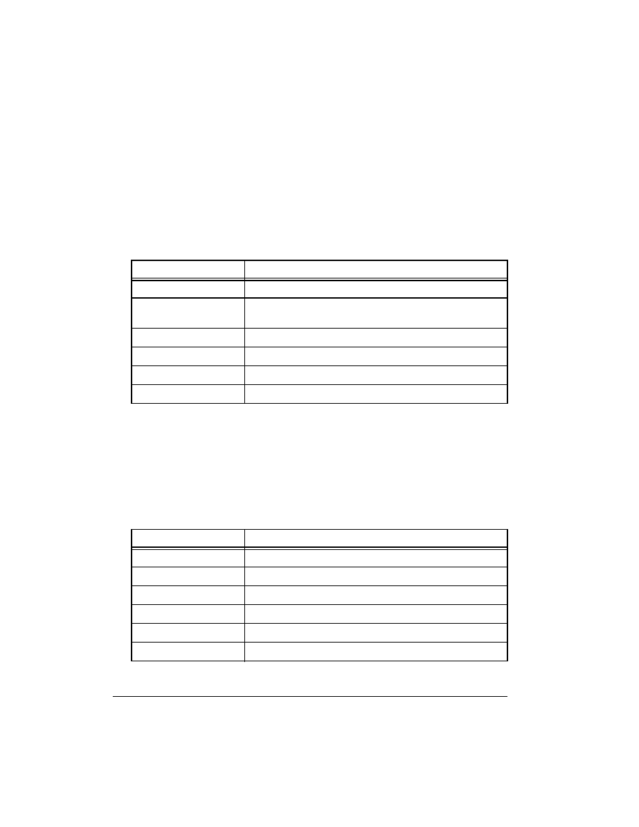 Push Buttons and Switches 2-8 ADSP-BF506F EZ-KIT Lite Evaluation System Manual UART Setup Switch (SW1) The UART setup switch (SW1) configures the UART0 signals between the DCE connector (J1) and processor. Table 2-5 shows the switch settings. Boot Mode Select Switch (SW2) The boot mode select switch (SW2) determines the boot mode of the pro- cessor. Table 2-5 shows the available boot mode settings. By default, the ADSP-BF506F processor boots from SPI flash memory. Table 2-4. UART Setup Switch (SW1) SW1 Position Function 1 and 3 Enable flow control 2 Disconnects the UART_RX signal from the processor; the UART_RX signal can be used for another function 4 Connects the RTS and CTS signals together 5 Allows the host to reset the EZ-KIT Lite via the CTS signal 6 and 7 Selects the source for the CTS signal 8 Loops the TX and RX signals together for testing Table 2-5. Boot Mode Select Switch (SW2) SW2 Position Processor Boot Mode 0 Idle—no boot 1 Boots from stacked parallel flash in asynchronous mode 2 Boots from stacked parallel flash in synchronous mode 3 Boots through SPI0 master from SPI memory 4 Boots through SPI0 slave from host device 5 Boots through PPI from host |
|
Link URL |
| Does ALLDATASHEET help your business so far? [ DONATE ] |
About Alldatasheet | Advertisement | Contact us | Privacy Policy | Link to Datasheet | Link Exchange | Manufacturer List All Rights Reserved©Alldatasheet.com |
| Russian : Alldatasheetru.com | Korean : Alldatasheet.co.kr | Spanish : Alldatasheet.es | French : Alldatasheet.fr | Italian : Alldatasheetit.com Portuguese : Alldatasheetpt.com | Polish : Alldatasheet.pl | Vietnamese : Alldatasheet.vn Indian : Alldatasheet.in | Mexican : Alldatasheet.com.mx | British : Alldatasheet.co.uk | New Zealand : Alldatasheet.co.nz |
|
Family Site : ic2ic.com |
icmetro.com |
 New Zealand ▼
 English
 Chinese
 German
 Japanese
 Russian
 Korean
 Spanish
 French
 Italian
 Portuguese
 Polish
 Vietnamese
 Indian
 Mexican
 British
 New Zealand


