 |
Electronic Components Datasheet Search |
|
|
Electronic Components Datasheet Search |
|
B3737 Datasheet(PDF) 5 Page - EPCOS |
|
|
|||||||||||||||||||||||||||||
B3737 Datasheet(HTML) 5 Page - EPCOS |
|
|
5 / 11 page 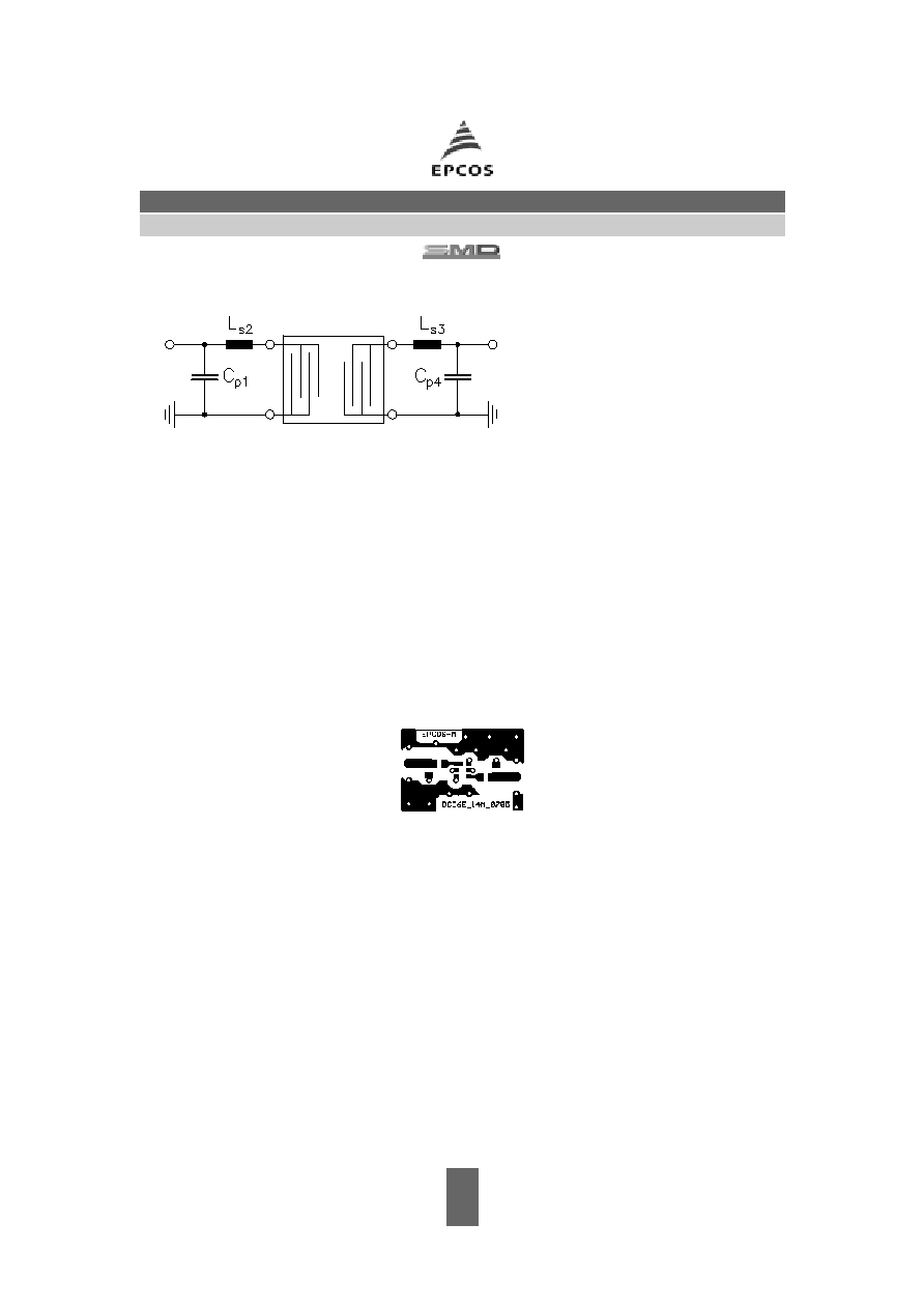 5 March 22, 2007 B3737 447.725 MHz SAW Components SAW filter Data sheet Please read cautions and warnings and important notes at the end of this document. Matching network to 50 Ω (element values depend on pcb layout and equivalent circuit) Minimising the crosstalk For a good ultimate rejection a low crosstalk is necessary. Low crosstalk can be realised with a good RF layout. The major crosstalk mechanism is caused by the “ground-loop” problem. Grounding loops are created if input-and output transducer GND are connected on the top-side of the PCB and fed to the system grounding plane by a common via hole. To avoid the common ground path, the ground pin of the input- and output transducer are fed to the system ground plane (bottom PCB plane) by their own via hole. The transducers’ grounding pins should be isolated from the upper grounding plane. A common GND inductivity of 0.5nH degrades the ultimate rejection (crosstalk) by 20dB. The optimised PCB layout, including matching network for transformation to 50 Ohm, is shown here. In this PCB layout the grounding loops are minimised to realise good ultimate rejection Optimised PCB layout for SAW filters in DCC6E package, pinning 1,4 (top side, scale 1:1) The bottom side is a copper plane (system ground area). The input and output grounding pins are isolated and connected to the common ground by separated via holes. For good contact of the upper grounding area with the lower side it is necessary to place enough via holes. Cp1 = 1.8 pF Ls2 = 39 nH Ls3 = 39 nH Cp4 = 1.8 pF |
|
|
Link URL |
| Does ALLDATASHEET help your business so far? [ DONATE ] |
About Alldatasheet | Advertisement | Contact us | Privacy Policy | Link to Datasheet | Link Exchange | Manufacturer List All Rights Reserved©Alldatasheet.com |
| Russian : Alldatasheetru.com | Korean : Alldatasheet.co.kr | Spanish : Alldatasheet.es | French : Alldatasheet.fr | Italian : Alldatasheetit.com Portuguese : Alldatasheetpt.com | Polish : Alldatasheet.pl | Vietnamese : Alldatasheet.vn Indian : Alldatasheet.in | Mexican : Alldatasheet.com.mx | British : Alldatasheet.co.uk | New Zealand : Alldatasheet.co.nz |
|
Family Site : ic2ic.com |
icmetro.com |
 New Zealand ▼
 English
 Chinese
 German
 Japanese
 Russian
 Korean
 Spanish
 French
 Italian
 Portuguese
 Polish
 Vietnamese
 Indian
 Mexican
 British
 New Zealand


