 |
Electronic Components Datasheet Search |
|
|
Electronic Components Datasheet Search |
|
XC161CS-32F Datasheet(PDF) 72 Page - Infineon Technologies AG |
|
|
|||||||||||||||||||||||||||||
XC161CS-32F Datasheet(HTML) 72 Page - Infineon Technologies AG |
|
|
72 / 87 page 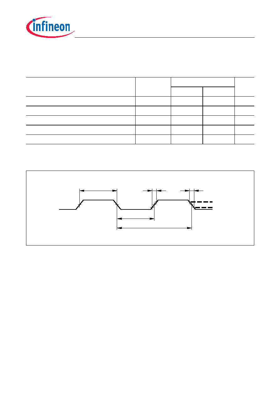 XC161CS-32F Derivatives Electrical Parameters Data Sheet 70 V1.2, 2006-08 4.4.3 External Clock Drive XTAL1 Figure 16 External Clock Drive XTAL1 Note: If the on-chip oscillator is used together with a crystal or a ceramic resonator, the oscillator frequency is limited to a range of 4 MHz to 16 MHz. It is strongly recommended to measure the oscillation allowance (negative resistance) in the final target system (layout) to determine the optimum parameters for the oscillator operation. Please refer to the limits specified by the crystal supplier. When driven by an external clock signal it will accept the specified frequency range. Operation at lower input frequencies is possible but is verified by design only (not subject to production test). Table 19 External Clock Drive Characteristics (Operating Conditions apply) Parameter Symbol Limit Values Unit Min. Max. Oscillator period t OSC SR 25 2501) 1) The maximum limit is only relevant for PLL operation to ensure the minimum input frequency for the PLL. ns High time2) 2) The clock input signal must reach the defined levels VILC and VIHC. t 1 SR 6–ns Low time2) t 2 SR 6–ns Rise time2) t 3 SR –8ns Fall time2) t 4 SR –8ns MCT05572 t 1 t 2 t OSC t 3 t 4 0.5 V DDI V ILC V IHC |
|
Link URL |
| Does ALLDATASHEET help your business so far? [ DONATE ] |
About Alldatasheet | Advertisement | Contact us | Privacy Policy | Link to Datasheet | Link Exchange | Manufacturer List All Rights Reserved©Alldatasheet.com |
| Russian : Alldatasheetru.com | Korean : Alldatasheet.co.kr | Spanish : Alldatasheet.es | French : Alldatasheet.fr | Italian : Alldatasheetit.com Portuguese : Alldatasheetpt.com | Polish : Alldatasheet.pl | Vietnamese : Alldatasheet.vn Indian : Alldatasheet.in | Mexican : Alldatasheet.com.mx | British : Alldatasheet.co.uk | New Zealand : Alldatasheet.co.nz |
|
Family Site : ic2ic.com |
icmetro.com |
 New Zealand ▼
 English
 Chinese
 German
 Japanese
 Russian
 Korean
 Spanish
 French
 Italian
 Portuguese
 Polish
 Vietnamese
 Indian
 Mexican
 British
 New Zealand


