|
Electronic Components Datasheet Search |
|
|
Electronic Components Datasheet Search |
|
RFHCS362F Datasheet(PDF) 21 Page - Microchip Technology |
|
|
|||||||||||||||||||||||||||||
RFHCS362F Datasheet(HTML) 21 Page - Microchip Technology |
|
|
21 / 54 page 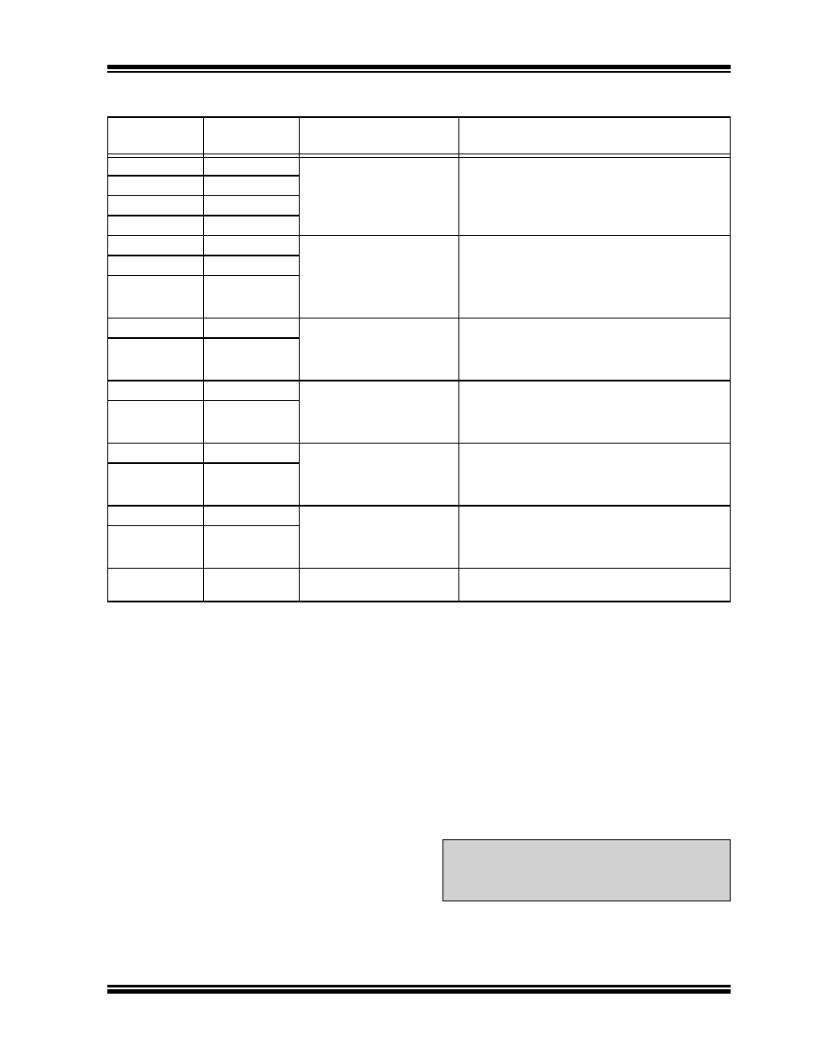 © 2011 Microchip Technology Inc. DS41189B-page 21 rfHCS362G/362F TABLE 4-2: CONFIG_0 4.5 Configuration Words There are 36 configuration bits stored in the EEPROM array. They are used by the device to determine trans- mission speed, format, delays and Guard times. They are grouped in three Configuration Words: CONFIG_0 , CONFIG_1 and the upper nybble of the SEED_3 word. A description of each of the bits follows this section. 4.5.1 OSC The internal oscillator can be tuned to ±10%. (0000 selects the nominal value, 1000 the fastest value and 0111 the slowest). When programming the device, it is the programmer’s responsibility to determine the opti- mal calibration value. 4.5.2 VLOW[0..2] The low voltage threshold can be programmed to be any of the values shown in Table 4-2. 4.5.3 BSEL[0..1] The basic timing element TE, determines the actual transmission Baud Rate. This translates to different code word lengths depending on the encoding format selected (Manchester or PWM), the Header length selection and the Guard time selection, from approxi- mately 40 ms up to 220 ms. Refer to Table 4-2 for bit rate configuration. Refer to Figure 10-3 through Figure 10-6 for code word timing. 4.5.4 MTX[0..1] MTX selects the minimum number of code words that will be transmitted. A minimum of 1, 2, 4 or 8 code words will be transmitted. Bit Address Field Description Values 0 OSC_0 Oscillator adjust 0000 - nominal 1000 - fastest 0111 - slowest 1 OSC_1 2 OSC_2 3 OSC_3 4 VLOW_0 VLOW select nominal values 5 VLOW_1 000 - 2.0V 001 - 2.1V 010 - 2.2V 011 - 2.3V 100 - 4.0V 101 - 4.2V 110 - 4.4V 111 - 4.6V 6 VLOW_2 7 BSEL_0 Bit rate select 00 - TE = 100 μs 01 - TE = 200 μs 10 - TE = 400 μs 11 - TE = 800 μs 8 BSEL_1 9 MTX_0 Minimum number of code words 00 - 1 01 - 2 10 - 4 11 - 8 10 MTX_1 11 GUARD_0 Guard time select 00 - 0 ms (1 TE) 01 - 6.4 ms + 2 TE 10 - 25.6 ms + 2 TE 11 - 76.8 ms + 2 TE 12 GUARD_1 13 TIMOUT_0 Time-out select 00 - No Time-out 01 - 0.8 s to 0.8 s + 1 code word 10 - 3.2 s to 3.2 s + 1 code word 11 - 25.6 s to 25.6 s + 1 code word 14 TIMOUT_1 15 CTSEL CTSEL 0 = TIME bits 1 = CRC bits Note: If MTX and BSEL settings in combination require a transmission sequence to exceed the TIMOUT setting, TIMOUT will take priority. |
|
Link URL |
| Does ALLDATASHEET help your business so far? [ DONATE ] |
About Alldatasheet | Advertisement | Contact us | Privacy Policy | Link to Datasheet | Link Exchange | Manufacturer List All Rights Reserved©Alldatasheet.com |
| Russian : Alldatasheetru.com | Korean : Alldatasheet.co.kr | Spanish : Alldatasheet.es | French : Alldatasheet.fr | Italian : Alldatasheetit.com Portuguese : Alldatasheetpt.com | Polish : Alldatasheet.pl | Vietnamese : Alldatasheet.vn Indian : Alldatasheet.in | Mexican : Alldatasheet.com.mx | British : Alldatasheet.co.uk | New Zealand : Alldatasheet.co.nz |
|
Family Site : ic2ic.com |
icmetro.com |
 New Zealand ▼
 English
 Chinese
 German
 Japanese
 Russian
 Korean
 Spanish
 French
 Italian
 Portuguese
 Polish
 Vietnamese
 Indian
 Mexican
 British
 New Zealand