|
Electronic Components Datasheet Search |
|
|
Electronic Components Datasheet Search |
|
P1580G-SH2-R Datasheet(PDF) 2 Page - Unisonic Technologies |
|
|
|||||||||||||||||||||||||||||
P1580G-SH2-R Datasheet(HTML) 2 Page - Unisonic Technologies |
|
|
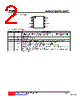
2 / 6 page 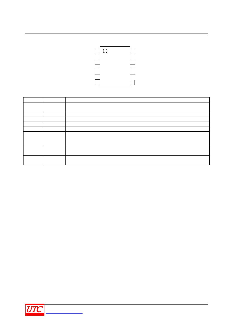 P1580 LINEAR INTEGRATED CIRCUIT UNISONICTECHNOLOGIESCO.,LTD 2 of 6 www.unisonic.com.tw QW-R103-049.A PIN CONFIGURATION 1 BS 2 IN 3 SW 8 SYNC 7 EN 6 COMP 5 FB GND 4 PIN DESCRIPTION PIN NO. PIN NAME DESCRIPTION 1 BS Supply pin to the power transistor driver. Tie to external circuit to generate a local supply voltage higher than the input voltage in order to fully turn on the internal power transistor. 2 IN Power Supply pin. 3 SW Power Switch Output pin. 4 GND Ground pin. 5 FB The output voltage feedback pin. It is also the inverting input of the error amplifier. 6 COMP Compensation pin. It is also the output of the internal error amplifier. (1). A RC network at this pin compensates the control loop. (2). The voltage at this pin controls the peak current of the internal switch. 7 EN Regulator On/Off Control pin. Leave EN unconnected if unused. A low input at EN turns on the converter, and a high input turns it off. 8 SYNC Synchronization Input - The sync pin is used to synchronize the internal oscillator to an external signal. |
|
|
Link URL |
| Does ALLDATASHEET help your business so far? [ DONATE ] |
About Alldatasheet | Advertisement | Contact us | Privacy Policy | Link to Datasheet | Link Exchange | Manufacturer List All Rights Reserved©Alldatasheet.com |
| Russian : Alldatasheetru.com | Korean : Alldatasheet.co.kr | Spanish : Alldatasheet.es | French : Alldatasheet.fr | Italian : Alldatasheetit.com Portuguese : Alldatasheetpt.com | Polish : Alldatasheet.pl | Vietnamese : Alldatasheet.vn Indian : Alldatasheet.in | Mexican : Alldatasheet.com.mx | British : Alldatasheet.co.uk | New Zealand : Alldatasheet.co.nz |
|
Family Site : ic2ic.com |
icmetro.com |
 New Zealand ▼
 English
 Chinese
 German
 Japanese
 Russian
 Korean
 Spanish
 French
 Italian
 Portuguese
 Polish
 Vietnamese
 Indian
 Mexican
 British
 New Zealand