|
Electronic Components Datasheet Search |
|
|
Electronic Components Datasheet Search |
|
ADL5303ACPZ-R2 Datasheet(PDF) 15 Page - Analog Devices |
|
|
|||||||||||||||||||||||||||||
ADL5303ACPZ-R2 Datasheet(HTML) 15 Page - Analog Devices |
|
|
15 / 24 page 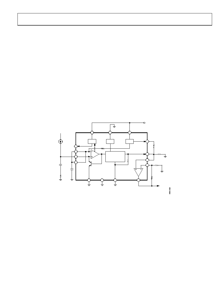 Data Sheet ADL5303 Rev. 0 | Page 15 of 24 LOW SUPPLY SLOPE AND INTERCEPT ADJUSTMENT When using the device with a supply of less than 4 V, it is necessary to reduce the slope and intercept at the VLOG pin to preserve good log conformance over the entire 160 dB oper- ating range. The voltage at the VLOG pin is generated by an internal current source with an output current of 40 μA/decade feeding the internal laser trimmed output resistance of 5 kΩ. When the voltage at the VLOG pin exceeds VP − 2.3 V, the current source ceases to respond linearly to logarithmic increases in current. Avoid headroom issues by reducing the logarithmic slope and intercept at the VLOG pin and by connecting an external resistor, RS, from the VLOG pin to ground in combination with an intercept lowering resistor, RZ. The values shown in Figure 28 illustrate a good solution for a 3.0 V positive supply. The resulting logarithmic slope measured at VLOG is 62.5 mV/decade with a new intercept of 57 fA. The original logarithmic slope of 200 mV/decade can be recovered using voltage gain on the internal buffer amplifier. CHANGING THE VOLTAGE AT THE SUMMING NODE The default value of VSUM is determined by using a quarter of VREF (2 V). This can be altered by applying an independent voltage source to VSUM, or by adding an external resistive divider from VREF to VSUM. This network operates in parallel with the internal divider (40 kΩ and 13.3 kΩ), and the choice of external resistors should take this into account. In practice, the total resistance of the added string may be as low as 10 kΩ (consuming 400 μA from VREF). Low values of VSUM and thus VCE are not advised when large values of IPD are expected. NC VOUT 500mV/DEC R18 (RB) C7 (RS) 2.67k Ω R14 (RZ) 15.4kΩ R15 (RA) 4.98k Ω 2.26k Ω NC = NO CONNECT VP 100nF R1 750 Ω C1 1nF IPD C3 PDB BIAS VREF VPDB VSUM INPT VSUM ACOM VPS2 PWDN VPS1 VREF VLOG BFIN BFNG VOUT 0.5V ADL5303 ~10k Ω 5kΩ 5 2 3 4 15 14 GND GND 7 11 10 16 12 6 8 9 13 TEMPERATURE COMPENSATION Figure 28. Recommended Low Supply Application Circuit |
|
|
Link URL |
| Does ALLDATASHEET help your business so far? [ DONATE ] |
About Alldatasheet | Advertisement | Contact us | Privacy Policy | Link to Datasheet | Link Exchange | Manufacturer List All Rights Reserved©Alldatasheet.com |
| Russian : Alldatasheetru.com | Korean : Alldatasheet.co.kr | Spanish : Alldatasheet.es | French : Alldatasheet.fr | Italian : Alldatasheetit.com Portuguese : Alldatasheetpt.com | Polish : Alldatasheet.pl | Vietnamese : Alldatasheet.vn Indian : Alldatasheet.in | Mexican : Alldatasheet.com.mx | British : Alldatasheet.co.uk | New Zealand : Alldatasheet.co.nz |
|
Family Site : ic2ic.com |
icmetro.com |
 New Zealand ▼
 English
 Chinese
 German
 Japanese
 Russian
 Korean
 Spanish
 French
 Italian
 Portuguese
 Polish
 Vietnamese
 Indian
 Mexican
 British
 New Zealand