 |
Electronic Components Datasheet Search |
|
|
Electronic Components Datasheet Search |
|
AD5360BSTZ1 Datasheet(PDF) 21 Page - Analog Devices |
|
|
|||||||||||||||||||||||||||||
AD5360BSTZ1 Datasheet(HTML) 21 Page - Analog Devices |
|
|
21 / 28 page 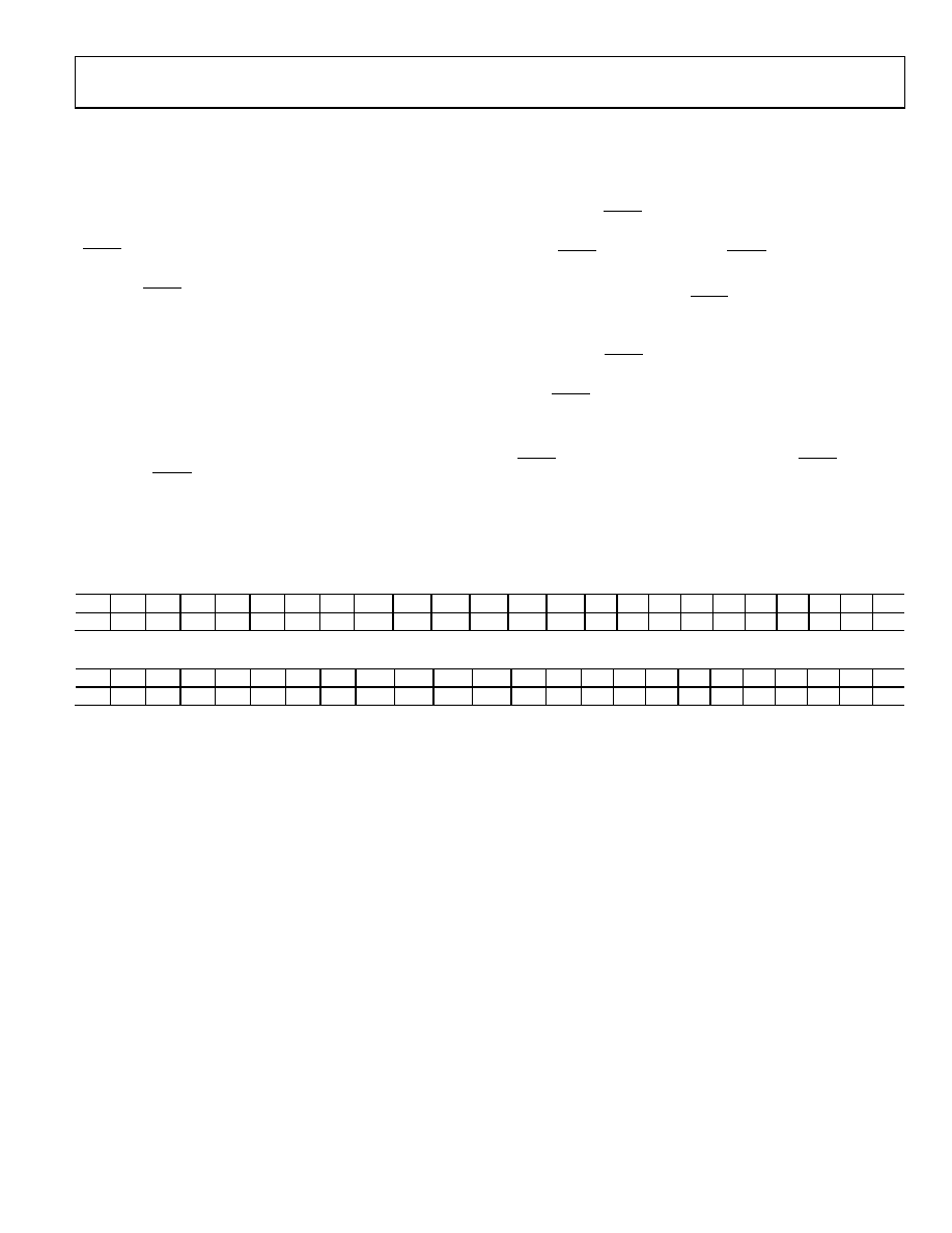 AD5360/AD5361 Rev. A | Page 21 of 28 SERIAL INTERFACE The AD5360/AD5361 contain a high speed SPI operating at clock frequencies up to 50 MHz (20 MHz for read operations). To minimize both the power consumption of the device and on-chip digital noise, the interface powers up fully only when the device is being written to, that is, on the falling edge of SYNC. The serial interface is 2.5 V LVTTL-compatible when operating from a 2.5 V to 3.6 V DVCC supply. It is controlled by four pins: SYNC (frame synchronization input), SDI (serial data input), SCLK (clocking of data in and out of the device), and SDO (serial data output for data readback). SPI WRITE MODE The AD5360/AD5361 allow writing of data via the serial inter- face to every register directly accessible to the serial interface, which are all registers except the X2A, X2B, and DAC registers. The X2A and X2B registers are updated when writing to the X1A, X1B, M, and C registers, and the DAC registers are updated by LDAC. The serial word (see or ) is 24 bits long; 16 or 14 of these bits are data bits, six bits are address bits, and two bits are mode bits that determine what is done with the data. Two bits are reserved on the AD5361. Table 10 Table 11 The serial interface works with both a continuous and a burst (gated) serial clock. Serial data applied to SDI is clocked into the AD5360/AD5361 by clock pulses applied to SCLK. The first falling edge of SYNC starts the write cycle. At least 24 falling clock edges must be applied to SCLK to clock in 24 bits of data, before SYNC is taken high again. If SYNC is taken high before the 24th falling clock edge, the write operation is aborted. If a continuous clock is used, SYNC must be taken high before the 25th falling clock edge. This inhibits the clock within the AD5360/AD5361. If more than 24 falling clock edges are applied before SYNC is taken high again, the input data is corrupted. If an externally gated clock of exactly 24 pulses is used, SYNC may be taken high any time after the 24th falling clock edge. The input register addressed is updated on the rising edge of SYNC. For another serial transfer to take place, SYNC must be taken low again. Table 10. AD5360 Serial Word Bit Assignation I23 I22 I21 I20 I19 I18 I17 I16 I15 I14 I13 I12 I11 I10 I9 I8 I7 I6 I5 I4 I3 I2 I1 I0 M1 M0 A5 A4 A3 A2 A1 A0 D15 D14 D13 D12 D11 D10 D9 D8 D7 D6 D5 D4 D3 D2 D1 D0 Table 11. AD5361 Serial Word Bit Assignation I23 I22 I21 I20 I19 I18 I17 I16 I15 I14 I13 I12 I11 I10 I9 I8 I7 I6 I5 I4 I3 I2 I11 I01 M1 M0 A5 A4 A3 A2 A1 A0 D13 D12 D11 D10 D9 D8 D7 D6 D5 D4 D3 D2 D1 D0 0 0 1 I1 and I0 are reserved for future use and should be 0 when writing the serial word. These bits read back as 0. |
|
Link URL |
| Does ALLDATASHEET help your business so far? [ DONATE ] |
About Alldatasheet | Advertisement | Contact us | Privacy Policy | Link to Datasheet | Link Exchange | Manufacturer List All Rights Reserved©Alldatasheet.com |
| Russian : Alldatasheetru.com | Korean : Alldatasheet.co.kr | Spanish : Alldatasheet.es | French : Alldatasheet.fr | Italian : Alldatasheetit.com Portuguese : Alldatasheetpt.com | Polish : Alldatasheet.pl | Vietnamese : Alldatasheet.vn Indian : Alldatasheet.in | Mexican : Alldatasheet.com.mx | British : Alldatasheet.co.uk | New Zealand : Alldatasheet.co.nz |
|
Family Site : ic2ic.com |
icmetro.com |
 New Zealand ▼
 English
 Chinese
 German
 Japanese
 Russian
 Korean
 Spanish
 French
 Italian
 Portuguese
 Polish
 Vietnamese
 Indian
 Mexican
 British
 New Zealand


