|
Electronic Components Datasheet Search |
|
|
Electronic Components Datasheet Search |
|
AD5665BCPZ-R2 Datasheet(PDF) 12 Page - Analog Devices |
|
|
|||||||||||||||||||||||||||||
AD5665BCPZ-R2 Datasheet(HTML) 12 Page - Analog Devices |
|
|
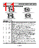
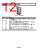
12 / 36 page 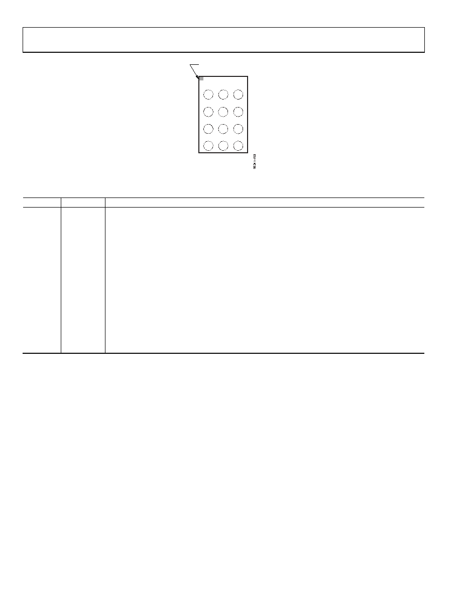 AD5625R/AD5645R/AD5665R, AD5625/AD5665 Data Sheet Rev. C | Page 12 of 36 Figure 8. Pin Configuration (12-Ball WLCSP) Table 8. Pin Function Descriptions Pin No. Mnemonic Description A1 VREFIN/VREFOUT The AD5665R has a common pin for reference input and reference output. When using the internal reference, this is the reference output pin. When using an external reference, this is the reference input pin. The default for this pin is as a reference input. A2, B2, C2 GND Ground Reference Point for All Circuitry on the Part. A3 VOUTA Analog Output Voltage from DAC A. The output amplifier has rail-to-rail operation. B1 VDD Power Supply Input. The AD5665R can be operated from 2.7 V to 5.5 V, and the supply should be decoupled with a 10 μF capacitor in parallel with a 0.1 μF capacitor to GND. B3 VOUTB Analog Output Voltage from DAC B. The output amplifier has rail-to-rail operation. C1 SDA Serial Data Line. This is used in conjunction with the SCL line to clock data into or out of the 16-bit input register. It is a bidirectional, open-drain data line that should be pulled to the supply with an external pull-up resistor. C3 VOUTC Analog Output Voltage from DAC C. The output amplifier has rail-to-rail operation. D1 SCL Serial Clock Line. This is used in conjunction with the SDA line to clock data into or out of the 16-bit input register. D2 ADDR Three-State Address Input. Sets the two least significant bits (Bit A1, Bit A0) of the 7-bit slave address (see Table 9). D3 VOUTD Analog Output Voltage from DAC D. The output amplifier has rail-to-rail operation. TOP VIEW (BALL SIDE DOWN) Not to Scale GND VOUTA VDD GND VOUTB SDA GND VOUTC SCL ADDR VOUTD 1 A B C D 2 3 BALL A1 INDICATOR VREFIN/ VREFOUT |
|
Link URL |
| Does ALLDATASHEET help your business so far? [ DONATE ] |
About Alldatasheet | Advertisement | Contact us | Privacy Policy | Link to Datasheet | Link Exchange | Manufacturer List All Rights Reserved©Alldatasheet.com |
| Russian : Alldatasheetru.com | Korean : Alldatasheet.co.kr | Spanish : Alldatasheet.es | French : Alldatasheet.fr | Italian : Alldatasheetit.com Portuguese : Alldatasheetpt.com | Polish : Alldatasheet.pl | Vietnamese : Alldatasheet.vn Indian : Alldatasheet.in | Mexican : Alldatasheet.com.mx | British : Alldatasheet.co.uk | New Zealand : Alldatasheet.co.nz |
|
Family Site : ic2ic.com |
icmetro.com |
 New Zealand ▼
 English
 Chinese
 German
 Japanese
 Russian
 Korean
 Spanish
 French
 Italian
 Portuguese
 Polish
 Vietnamese
 Indian
 Mexican
 British
 New Zealand