 |
Electronic Components Datasheet Search |
|
|
Electronic Components Datasheet Search |
|
ADP1720ARMZ-5-R7 Datasheet(PDF) 14 Page - Analog Devices |
|
|
|||||||||||||||||||||||||||||
ADP1720ARMZ-5-R7 Datasheet(HTML) 14 Page - Analog Devices |
|
|
14 / 16 page 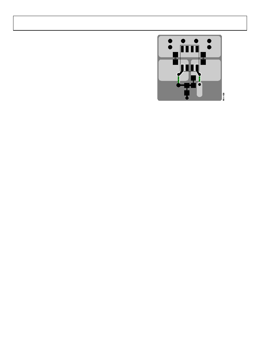 ADP1720 Rev. A | Page 14 of 16 PRINTED CIRCUIT BOARD LAYOUT CONSIDERATIONS R1 C2 C1 ADP1720 IN OUT GND (TOP) R2 EN GND (BOTTOM) Heat dissipation from the package can be improved by increasing the amount of copper attached to the pins of the ADP1720. How- ever, as can be seen from Table 5, a point of diminishing returns eventually is reached, beyond which an increase in the copper size does not yield significant heat dissipation benefits. Place the input capacitor as close as possible to the IN and GND pins. Place the output capacitor as close as possible to the OUT and GND pins. Use of 0402 or 0603 size capacitors and resistors achieves the smallest possible footprint solution on boards where area is limited. Figure 28. Example PCB Layout |
|
|
Link URL |
| Does ALLDATASHEET help your business so far? [ DONATE ] |
About Alldatasheet | Advertisement | Contact us | Privacy Policy | Link to Datasheet | Link Exchange | Manufacturer List All Rights Reserved©Alldatasheet.com |
| Russian : Alldatasheetru.com | Korean : Alldatasheet.co.kr | Spanish : Alldatasheet.es | French : Alldatasheet.fr | Italian : Alldatasheetit.com Portuguese : Alldatasheetpt.com | Polish : Alldatasheet.pl | Vietnamese : Alldatasheet.vn Indian : Alldatasheet.in | Mexican : Alldatasheet.com.mx | British : Alldatasheet.co.uk | New Zealand : Alldatasheet.co.nz |
|
Family Site : ic2ic.com |
icmetro.com |
 New Zealand ▼
 English
 Chinese
 German
 Japanese
 Russian
 Korean
 Spanish
 French
 Italian
 Portuguese
 Polish
 Vietnamese
 Indian
 Mexican
 British
 New Zealand


