 |
Electronic Components Datasheet Search |
|
|
Electronic Components Datasheet Search |
|
4066G-P14-R Datasheet(PDF) 5 Page - Unisonic Technologies |
|
|
|||||||||||||||||||||||||||||
4066G-P14-R Datasheet(HTML) 5 Page - Unisonic Technologies |
|
|
5 / 7 page 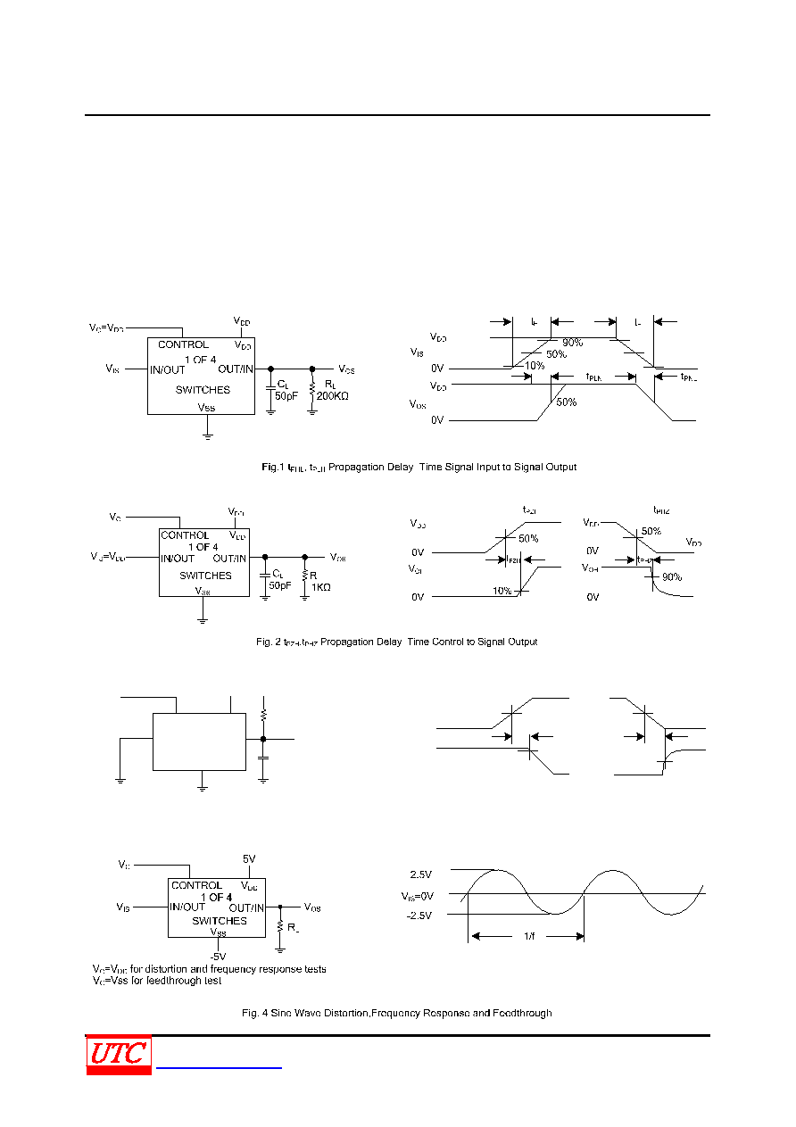 4066 CMOS IC UNISONICTECHNOLOGIESCO.,LTD 5 of 7 www.unisonic.com.tw QW-R502-009.F SPECIAL CONSIDERATIONS In applications where separate power sources are used to drive VDD and the signal input, the VDD current capability should exceed VDD/RL (RL=effective external load of the UTC 4066 bilateral switches).This provision avoids any permanent current flow or clamp action of the VDD supply when power is applied or removed from UTC 4066. In certain applications, the external load-resistor current may include both VDD and Signal-line components. To avoid drawing VDD current when switch current flows into terminals 1,4,8 or 11,the voltage drop across the bidirectional swith must not exceed 0.6V at TA ≤ 25°C, or 0.4V at TA >25°C (calculated from RON values shown). NO VDD current will flow through RL if the switch current flows into terminals2, 3, 9 or 10. AC TEST CIRCUITS AND SWITCHING TIME WAVEFORMS CONTROL VDD IN/OUT OUT/IN VSS 1 OF 4 SWITCHES VC VDD VOS RL 1KΩ 50% VDD 0V VDD VOL tPLZ Fig. 3 tPZL,tPLZ Propagation Delay Time Control to Signal Output VIS=0V tPZL VDD 0V 50% tPZL tPLZ VDD 90% 10% VDD VOL CL 50pF |
|
|
Link URL |
| Does ALLDATASHEET help your business so far? [ DONATE ] |
About Alldatasheet | Advertisement | Contact us | Privacy Policy | Link to Datasheet | Link Exchange | Manufacturer List All Rights Reserved©Alldatasheet.com |
| Russian : Alldatasheetru.com | Korean : Alldatasheet.co.kr | Spanish : Alldatasheet.es | French : Alldatasheet.fr | Italian : Alldatasheetit.com Portuguese : Alldatasheetpt.com | Polish : Alldatasheet.pl | Vietnamese : Alldatasheet.vn Indian : Alldatasheet.in | Mexican : Alldatasheet.com.mx | British : Alldatasheet.co.uk | New Zealand : Alldatasheet.co.nz |
|
Family Site : ic2ic.com |
icmetro.com |
 New Zealand ▼
 English
 Chinese
 German
 Japanese
 Russian
 Korean
 Spanish
 French
 Italian
 Portuguese
 Polish
 Vietnamese
 Indian
 Mexican
 British
 New Zealand


