 |
Electronic Components Datasheet Search |
|
|
Electronic Components Datasheet Search |
|
UCD7138DRST Datasheet(PDF) 21 Page - Texas Instruments |
|
|
|
|||||||||||||||||||||||||||||
UCD7138DRST Datasheet(HTML) 21 Page - Texas Instruments |
|
|
21 / 36 page 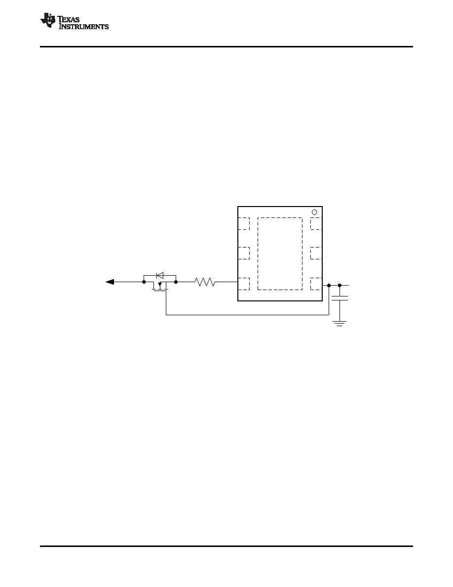 1 2 3 6 4 5 Thermal Pad (GND) CTRL DTC IN VD OUT VCC UCD7138 Connect to SR MOSFET drain terminal G D S UCD7138 www.ti.com SLVSCS1B – MARCH 2015 – REVISED MAY 2015 Typical Application (continued) 9.2.1.1.3 Drain-to-Source Voltage Sensing When the drain-to-source voltage is below 0 V, current flows out of the VD pin to the drain terminal of the MOSFET. This current flow must be limited to ensure proper operation of the device. The recommended current- limiting resistance value is 20 Ω. The highest voltage that can be applied to VD pin is 45 V which is good for applications where 40-V MOSFETs are used for the secondary-side SRs. If a higher voltage is required for VD pin, an external high-voltage blocking circuit can be used together with the UCD7138 device as shown in Figure 34. Depending on the required voltage rating, a different external high-voltage blocking MOSFET can be selected. Usually a small SOT-23 MOSFET can be used. In this circuit, the gate terminal of the external high-voltage blocking MOSFET is connected to VCC of the UCD7138 gate driver. The source terminal is connected with a current-limiting resistor to the VD pin of the UCD7138 device. The drain terminal is connected to the SR MOSFET drain terminal. When a low voltage is presented at the drain terminal, the blocking MOSFET is turned on because of the positive gate-to-source voltage. When the drain voltage becomes higher and higher, the source terminal voltage rises along with the drain terminal until the gate-to-source voltage falls below the threshold. When the source voltage is high enough so that the blocking MOSFET is turned off, the high voltage on the SR drain is blocked. Figure 34. External High-Voltage Blocking Circuit 9.2.1.1.4 DTC Output The DTC pin is the internal comparator output. This pin should be connected to the DTC0 or DTC1 pin on the UCD3138A device. To keep edges sharp, no filtering is recommended. If noise spikes are observed on the DTC signal, the blanking times in the UCD3138A device can be used to prevent the digital controller from sensing noise. This pin is not designed to drive large current. If filtering must be used, ensure that the sink and source current on this pin is within ±4 mA as specified in the Electrical Characteristics table. 9.2.1.1.5 Turn-on Edge Optimization The turnon edge optimization is useful when a positive current flow is at the rising edge of SRs. To maximize the efficiency gain, the dead time between the falling edge of the primary and the rising edge of the secondary should be programmed to a smaller value than expected, so that the rising edge of the SRs can move freely by UCD7138. 9.2.1.2 Detailed Design Procedure 9.2.1.2.1 Design Without SR-Control Optimization The design procedure of an LLC converter with synchronous rectification can be greatly simplified by using the UCD7138 and UCD3138A chipset. The converter hardware and firmware can initially be designed without advanced SR optimization and then add SR optimization function in. Copyright © 2015, Texas Instruments Incorporated Submit Documentation Feedback 21 Product Folder Links: UCD7138 |
|
Link URL |
| Does ALLDATASHEET help your business so far? [ DONATE ] |
About Alldatasheet | Advertisement | Contact us | Privacy Policy | Link to Datasheet | Link Exchange | Manufacturer List All Rights Reserved©Alldatasheet.com |
| Russian : Alldatasheetru.com | Korean : Alldatasheet.co.kr | Spanish : Alldatasheet.es | French : Alldatasheet.fr | Italian : Alldatasheetit.com Portuguese : Alldatasheetpt.com | Polish : Alldatasheet.pl | Vietnamese : Alldatasheet.vn Indian : Alldatasheet.in | Mexican : Alldatasheet.com.mx | British : Alldatasheet.co.uk | New Zealand : Alldatasheet.co.nz |
|
Family Site : ic2ic.com |
icmetro.com |
 New Zealand ▼
 English
 Chinese
 German
 Japanese
 Russian
 Korean
 Spanish
 French
 Italian
 Portuguese
 Polish
 Vietnamese
 Indian
 Mexican
 British
 New Zealand


