 |
Electronic Components Datasheet Search |
|
|
Electronic Components Datasheet Search |
|
USB5742-/2G Datasheet(PDF) 13 Page - Microchip Technology |
|
|
|||||||||||||||||||||||||||||
USB5742-/2G Datasheet(HTML) 13 Page - Microchip Technology |
|
|
13 / 46 page 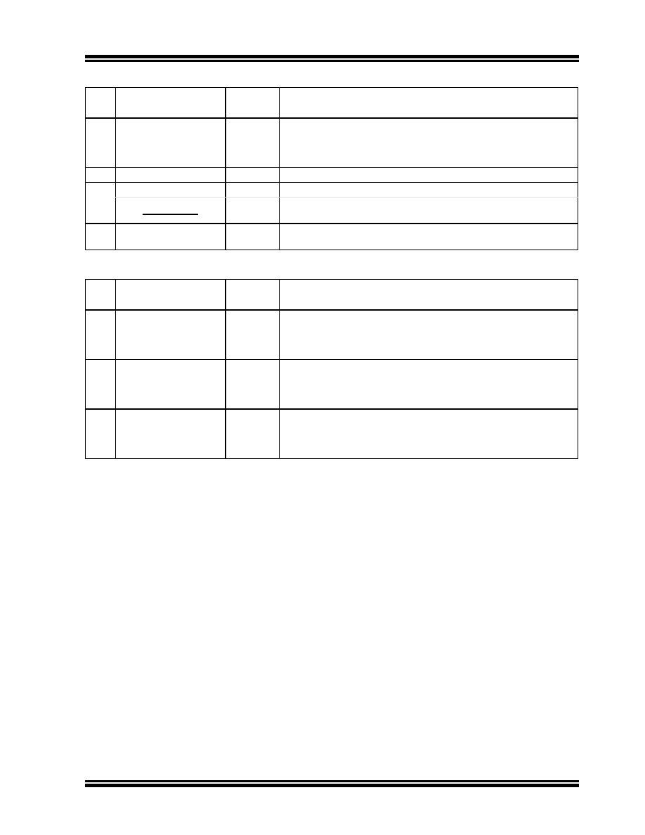 2015-2016 Microchip Technology Inc. DS00002016B-page 13 USB5742 1 ATEST AI Analog test pin. This signal is used for test purposes and must always be connected to ground. 1 GPIO19 I/O6 General purpose input/output 19. 1 GPIO20 I/O6 General purpose input/output 20. GANG_PWR I (PU) When pulled high enables gang mode. Gang power pin when used in gang mode. 12 NC - No Connect. These pins must be left unconnected for proper opera- tion. TABLE 3-7: POWER AND GROUND PIN DESCRIPTIONS Num Pins Symbol Buffer Type Description 4 VDD33 P +3.3 V power and internal regulator input Refer to Section 4.1, "Power Connections" for power connection infor- mation. 8 VDD12 P +1.2 V core power Refer to Section 4.1, "Power Connections" for power connection infor- mation. Pad VSS P Common ground. This exposed pad must be connected to the ground plane with a via array. TABLE 3-6: MISCELLANEOUS PIN DESCRIPTIONS (CONTINUED) Num Pins Symbol Buffer Type Description |
|
Link URL |
| Does ALLDATASHEET help your business so far? [ DONATE ] |
About Alldatasheet | Advertisement | Contact us | Privacy Policy | Link to Datasheet | Link Exchange | Manufacturer List All Rights Reserved©Alldatasheet.com |
| Russian : Alldatasheetru.com | Korean : Alldatasheet.co.kr | Spanish : Alldatasheet.es | French : Alldatasheet.fr | Italian : Alldatasheetit.com Portuguese : Alldatasheetpt.com | Polish : Alldatasheet.pl | Vietnamese : Alldatasheet.vn Indian : Alldatasheet.in | Mexican : Alldatasheet.com.mx | British : Alldatasheet.co.uk | New Zealand : Alldatasheet.co.nz |
|
Family Site : ic2ic.com |
icmetro.com |
 New Zealand ▼
 English
 Chinese
 German
 Japanese
 Russian
 Korean
 Spanish
 French
 Italian
 Portuguese
 Polish
 Vietnamese
 Indian
 Mexican
 British
 New Zealand


