|
Electronic Components Datasheet Search |
|
|
Electronic Components Datasheet Search |
|
U490B Datasheet(PDF) 2 Page - TEMIC Semiconductors |
|
|
|||||||||||||||||||||||||||||
U490B Datasheet(HTML) 2 Page - TEMIC Semiconductors |
|
|
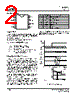
2 / 6 page  U490B TELEFUNKEN Semiconductors Rev. A1, 29-May-96 2 (6) Pin Description 1 2 3 4 5 6 7 8 NC Trigger Sync. GND VS Ramp Output Contr Pin Symbol Function 1 NC Not connected 2 Trigger Triggering 3 Sync. Synchronization 4 GND Ground 5 Contr Control input 6 Ramp Ramp 7 Output Output 8 VS Supply voltage Supply, Pin 8 Internal voltage limiter enables a simple supply from the mains via series resistor R1.The supply voltage between Pin 8 (VS) and ground (Pin 4) builts up via R1 and is smoothed by the capacitor C1. Series resistor R1 can be calculated as follows: R 1max [ 0.85 x V mains –VSmax 2xItot where Vmains + Mains supply voltage VSmax + Maximum supply voltage Itot + ISmax )IX ISmax + Maximum current consumption of the IC IX + Current consumption of the external components Phase Control, Pins 3, 5 and 6 The circuit is synchronized with mains supply through Pin 3. As long as the switch S1 is open, the circuit is in wait state i.e., the capacitor C6 (150 nF) is discharged and is kept in this state (High level). When the switch S1 is closed, there is a current flow in Pin 2 which is evaluated by the circuit. If this current flows after the elapse of delay time, then the phase control is released. Capacitor, C6, is then charged with I6 + 100 mA towards ground. At the same time, there is a current flow of [ 100 mA into Pin 5, which results in voltage drop across resistor R5. Control voltage, V5, is then 1.5 V lower internally. The output stage is released when the ramp voltage V6 is equal to (V5 * 1.5 V). When the voltage difference is [ 150 mV, it is again turned–off. The result is an output pulse, whose phase shift to the zero crossing of mains voltage is determined by the resistor R5 at control input Pin 5 (see fig. 2). Capacitor C6 is charged to a value of [ 1.5 V. It remains there till the switch S1 again opens and the repetition delay time is over. The circuit is released, when four periods of the line volt- age have expired after build up of the operating voltage, before the switch S1 is closed. closed open V8 V8 S1 V3 (Sync.) V2 (Trigger) V6 (Ramp) (Output) 0 50 ms 100 ms 150 ms 200 ms t V6 V7 t 150 mV ”X” ”X” 95 10867 t1 V5 – 1.5 V V7 tp Figure 2. Signal characteristics |
|
|
Link URL |
| Does ALLDATASHEET help your business so far? [ DONATE ] |
About Alldatasheet | Advertisement | Contact us | Privacy Policy | Link to Datasheet | Link Exchange | Manufacturer List All Rights Reserved©Alldatasheet.com |
| Russian : Alldatasheetru.com | Korean : Alldatasheet.co.kr | Spanish : Alldatasheet.es | French : Alldatasheet.fr | Italian : Alldatasheetit.com Portuguese : Alldatasheetpt.com | Polish : Alldatasheet.pl | Vietnamese : Alldatasheet.vn Indian : Alldatasheet.in | Mexican : Alldatasheet.com.mx | British : Alldatasheet.co.uk | New Zealand : Alldatasheet.co.nz |
|
Family Site : ic2ic.com |
icmetro.com |
 New Zealand ▼
 English
 Chinese
 German
 Japanese
 Russian
 Korean
 Spanish
 French
 Italian
 Portuguese
 Polish
 Vietnamese
 Indian
 Mexican
 British
 New Zealand