|
Electronic Components Datasheet Search |
|
|
Electronic Components Datasheet Search |
|
AD8557ACPZ-R2 Datasheet(PDF) 7 Page - Analog Devices |
|
|
|||||||||||||||||||||||||||||
AD8557ACPZ-R2 Datasheet(HTML) 7 Page - Analog Devices |
|
|
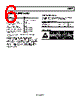
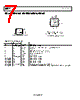
7 / 25 page 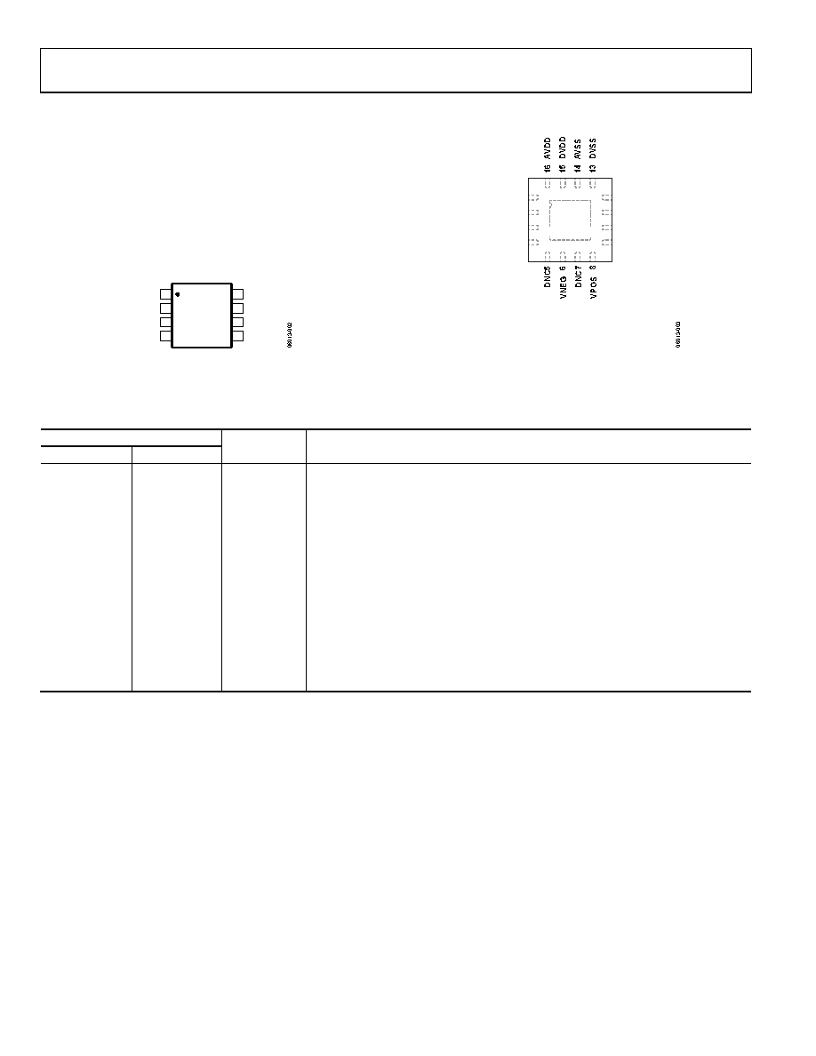 AD8557 Data Sheet Rev. D | Page 6 of 24 PIN CONFIGURATIONS AND FUNCTION DESCRIPTIONS VSS 8 VOUT 7 VCLAMP 6 VPOS 5 VDD 1 DIGOUT 2 DIGIN 3 VNEG 4 AD8557 TOP VIEW (Not to Scale) Figure 2. 8-Lead SOIC Pin Configuration NOTES 1. THE EXPOSED PAD SHOULD BE CONNECTED TO AVSS (PIN 14) OR LEFT UNCONNECTED. 2. DNC = DO NOT CONNECT. 12 11 10 1 3 49 2 DNC DIGOUT DNC DIGIN VOUT DNC VCLAMP DNC AD8557 TOP VIEW (Not to Scale) Figure 3. 16-Lead LFCSP Pin Configuration Table 5. Pin Function Descriptions Pin No. Mnemonic Description SOIC LFCSP 1 Not applicable VDD Positive Supply Voltage. 2 2 DIGOUT Digital Output. In read mode, this pin functions as a digital output. 3 4 DIGIN Digital Input. 4 6 VNEG Negative Amplifier Input (Inverting Input). 5 8 VPOS Positive Amplifier Input (Noninverting Input). 6 10 VCLAMP Set Clamp Voltage at Output. 7 12 VOUT Amplifier Output. 8 Not applicable VSS Negative Supply Voltage. Not applicable 13 DVSS Negative Supply Voltage. Not applicable 14 AVSS Negative Supply Voltage. Not applicable 15 DVDD Positive Supply Voltage. Not applicable 16 AVDD Positive Supply Voltage. Not applicable 1, 3, 5, 7, 9, 11 DNC Do Not Connect. Do not connect to these pins. Not applicable 0 EPAD Exposed Pad. The exposed pad should be connected to AVSS (Pin 14) or left unconnected. |
|
|
Link URL |
| Does ALLDATASHEET help your business so far? [ DONATE ] |
About Alldatasheet | Advertisement | Contact us | Privacy Policy | Link to Datasheet | Link Exchange | Manufacturer List All Rights Reserved©Alldatasheet.com |
| Russian : Alldatasheetru.com | Korean : Alldatasheet.co.kr | Spanish : Alldatasheet.es | French : Alldatasheet.fr | Italian : Alldatasheetit.com Portuguese : Alldatasheetpt.com | Polish : Alldatasheet.pl | Vietnamese : Alldatasheet.vn Indian : Alldatasheet.in | Mexican : Alldatasheet.com.mx | British : Alldatasheet.co.uk | New Zealand : Alldatasheet.co.nz |
|
Family Site : ic2ic.com |
icmetro.com |
 New Zealand ▼
 English
 Chinese
 German
 Japanese
 Russian
 Korean
 Spanish
 French
 Italian
 Portuguese
 Polish
 Vietnamese
 Indian
 Mexican
 British
 New Zealand