 |
Electronic Components Datasheet Search |
|
|
Electronic Components Datasheet Search |
|
ATSAM9708 Datasheet(PDF) 19 Page - ATMEL Corporation |
|
|
|||||||||||||||||||||||||||||
ATSAM9708 Datasheet(HTML) 19 Page - ATMEL Corporation |
|
|
19 / 30 page 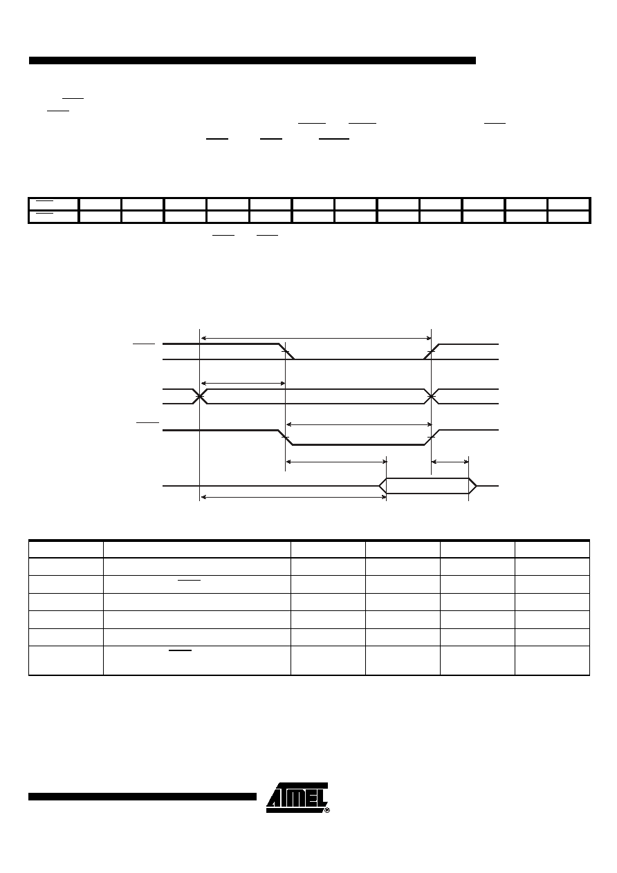 19 ATSAM9708 1772D–DRMSD–01/04 •As RAS only counter refresh method is employed, several banks of DRAMs can be connected using simple external CAS decoding. Linear address lines (WAx) can be used to select between DRAM banks. For example, a 1M x 32 SIMM module may be connected as two 1M x 16 banks, with CAS0 and CAS1 selections issued from CAS and WA20. • During a whole DRAM cycle (from RAS low to CAS rising), WCS0 is asserted low. • The equivalence between multiplexed DRAM address lines (DRA0 to DRA11) and the corresponding linear addressing (WA0 to WA23) is as follows: • To save DRAM power consumption, CAS and RAS are cycled only when necessary. Therefore, depending on firmware loaded, total board power consumption may increase with synthesis processing traffic. Detailed External ROM Timing Figure 12. ROM Read Cycle DRA11 DRA10 DRA9 DRA8 DRA7 DRA6 DRA5 DRA4 DRA3 DRA2 DRA1 DRA0 RAS time WA22 WA20 WA18 WA8 WA7 WA6 WA5 WA4 WA3 WA2 WA1 WA0 CAS time WA23 WA21 WA19 WA17 WA16 WA15 WA14 WA13 WA12 WA11 WA10 WA9 Table 13. External ROM Timing Parameters Symbol Parameter Min Typ Max Unit t RC Read cycle time 6 x t CK ns t AOE Address valid to WOE low t CK ns t POE Output enable pulse width 5 x t ck ns t AD Address access time 6 x t CK - 5 ns t OE Output enable access time 5 x t CK - 5 ns t DF Chip select or WOE high to input data High Z 0t CK - 5 ns tRC tAOE tPOE tOE tAD tDF WA[26:0] WD[15:0] WCS0 WOE |
|
Link URL |
| Does ALLDATASHEET help your business so far? [ DONATE ] |
About Alldatasheet | Advertisement | Contact us | Privacy Policy | Link to Datasheet | Link Exchange | Manufacturer List All Rights Reserved©Alldatasheet.com |
| Russian : Alldatasheetru.com | Korean : Alldatasheet.co.kr | Spanish : Alldatasheet.es | French : Alldatasheet.fr | Italian : Alldatasheetit.com Portuguese : Alldatasheetpt.com | Polish : Alldatasheet.pl | Vietnamese : Alldatasheet.vn Indian : Alldatasheet.in | Mexican : Alldatasheet.com.mx | British : Alldatasheet.co.uk | New Zealand : Alldatasheet.co.nz |
|
Family Site : ic2ic.com |
icmetro.com |
 New Zealand ▼
 English
 Chinese
 German
 Japanese
 Russian
 Korean
 Spanish
 French
 Italian
 Portuguese
 Polish
 Vietnamese
 Indian
 Mexican
 British
 New Zealand


