 |
Electronic Components Datasheet Search |
|
|
Electronic Components Datasheet Search |
|
The question interval is too short.
Please try again in a few seconds.

Hello, Please ask a question about BSN012N03LSI Datasheet
# Example questions:
➢ What disclaimer does infineon technologies make regarding the use of their components in life-support devices?
➢ What does the document not guarantee?
➢ What is the lg-uson-6-1?
| Part No. | BSN012N03LSI |
| Manufacturer | INFINEON |
| Size | 509 Kbytes |
| Pages | 9 pages |
| Description | Optimized for high performance Buck converter |


1. Device Overview
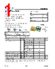
️· Device Name: BSN012N03LSI
️· Type: MOSFET (likely a power MOSFET, judging by the data provided)
️· Package: LG-USON-6-1 (A small, surface-mount package)
️· Manufacturer: Infineon Technologies AG
️· Document Revision: Rev. 2.0
️· Date: 2014-05-23
2. Electrical Characteristics (Extracted from Graphs and Tables - Incomplete due to image quality/resolution, but key points identified)
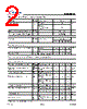
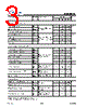
️· Drain-Source Voltage (Vds): Indicates the maximum voltage that can be applied between the drain and source terminals. Based on graphs, this appears to be significant, likely upwards of 30V.
️· Gate-Source Voltage (Vgs): Specifies the voltage range allowed between the gate and source terminals.
️· Drain Current (Id): The amount of current the MOSFET can handle.
️· Threshold Voltage (gs(th)): The gate voltage required to turn the MOSFET *on*.
️· Gate Charge (Qg): A measure of the total charge required to fully turn on the MOSFET.
️· Leakage Current (I DSS): The current that flows when the MOSFET is supposed to be "off." This is minimal but still a parameter.
️· RDS(on): Drain-Source on-resistance. A crucial parameter for efficiency - lower RDS(on) means less power loss. Not explicitly stated, but graphs hint at low values at specific Vgs values.
3. Key Graphs & Plots (Descriptions)
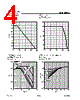
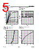
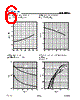
️· Drain Current vs. Gate-Source Voltage: Shows how the drain current changes as the gate voltage increases. This illustrates the MOSFET's turn-on characteristic.
️· Drain Current vs. Drain-Source Voltage: Illustrates the device's ability to handle voltages.
️· Threshold Voltage vs. Temperature: Shows how the turn-on voltage changes with temperature.
️· Gate Charge vs. Gate-Source Voltage: Depicts the gate charge as a function of the gate voltage.
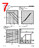
️· Avalanche Characteristics: Shows the device's behavior under avalanche conditions (a potentially destructive regime).
️· Gate Charge Waveforms: Illustrates the timing and shape of the gate charge during switching.
️· Leakage Current vs. Temperature: Plots the leakage current with temperature changes.
4. Avalanche Characteristics
️· `IAS`: Avalanche Current - The maximum current the device can handle during an avalanche event.
️· `tAV`: Avalanche Time - The duration of the avalanche condition.
5. Gate Charge Waveforms
️· `Qg`: Total gate charge (used to switch the device)
️· `Qgs`: Gate charge at source terminal.
️· `Qgd`: Gate charge at drain terminal.
6. Package Information
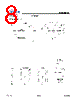
️· LG-USON-6-1: A small outline package. Precise dimensions are on a separate page (page 8).
7. Legal and Disclaimer
️· Standard legal disclaimers regarding device warranties, usage in life-support systems, and potential hazardous substances.
Important Notes and Limitations
️· Image Quality: This analysis is based on text that's difficult to read. Some numerical values are estimates based on trends and scales. A high-quality PDF of the datasheet would be significantly better for extracting accurate data.
️· Incomplete Data: This is *not* a complete datasheet. Many other parameters are likely present in the full document.
️· Context is Key: The specifications (Vds, Id, RDS(on)) will vary greatly depending on the gate voltage (Vgs) and temperature. The datasheet provides graphs to illustrate these dependencies.
1. Device Overview
️· Device Name: BSN012N03LSI
️· Type: MOSFET (likely a power MOSFET, judging by the data provided)
️· Package: LG-USON-6-1 (A small, surface-mount package)
️· Manufacturer: Infineon Technologies AG
️· Document Revision: Rev. 2.0
️· Date: 2014-05-23
2. Electrical Characteristics (Extracted from Graphs and Tables - Incomplete due to image quality/resolution, but key points identified)
️· Drain-Source Voltage (Vds): Indicates the maximum voltage that can be applied between the drain and source terminals. Based on graphs, this appears to be significant, likely upwards of 30V.
️· Gate-Source Voltage (Vgs): Specifies the voltage range allowed between the gate and source terminals.
️· Drain Current (Id): The amount of current the MOSFET can handle.
️· Threshold Voltage (gs(th)): The gate voltage required to turn the MOSFET *on*.
️· Gate Charge (Qg): A measure of the total charge required to fully turn on the MOSFET.
️· Leakage Current (I DSS): The current that flows when the MOSFET is supposed to be "off." This is minimal but still a parameter.
️· RDS(on): Drain-Source on-resistance. A crucial parameter for efficiency - lower RDS(on) means less power loss. Not explicitly stated, but graphs hint at low values at specific Vgs values.
3. Key Graphs & Plots (Descriptions)
️· Drain Current vs. Gate-Source Voltage: Shows how the drain current changes as the gate voltage increases. This illustrates the MOSFET's turn-on characteristic.
️· Drain Current vs. Drain-Source Voltage: Illustrates the device's ability to handle voltages.
️· Threshold Voltage vs. Temperature: Shows how the turn-on voltage changes with temperature.
️· Gate Charge vs. Gate-Source Voltage: Depicts the gate charge as a function of the gate voltage.
️· Avalanche Characteristics: Shows the device's behavior under avalanche conditions (a potentially destructive regime).
️· Gate Charge Waveforms: Illustrates the timing and shape of the gate charge during switching.
️· Leakage Current vs. Temperature: Plots the leakage current with temperature changes.
4. Avalanche Characteristics
️· `IAS`: Avalanche Current - The maximum current the device can handle during an avalanche event.
️· `tAV`: Avalanche Time - The duration of the avalanche condition.
5. Gate Charge Waveforms
️· `Qg`: Total gate charge (used to switch the device)
️· `Qgs`: Gate charge at source terminal.
️· `Qgd`: Gate charge at drain terminal.
6. Package Information
️· LG-USON-6-1: A small outline package. Precise dimensions are on a separate page (page 8).
7. Legal and Disclaimer
️· Standard legal disclaimers regarding device warranties, usage in life-support systems, and potential hazardous substances.
Important Notes and Limitations
️· Image Quality: This analysis is based on text that's difficult to read. Some numerical values are estimates based on trends and scales. A high-quality PDF of the datasheet would be significantly better for extracting accurate data.
️· Incomplete Data: This is *not* a complete datasheet. Many other parameters are likely present in the full document.
️· Context is Key: The specifications (Vds, Id, RDS(on)) will vary greatly depending on the gate voltage (Vgs) and temperature. The datasheet provides graphs to illustrate these dependencies.
| Part No. | BSN012N03LSI |
| Manufacturer | INFINEON |
| Size | 509 Kbytes |
| Pages | 9 pages |
| Description | Optimized for high performance Buck converter |
| Does ALLDATASHEET help your business so far? [ DONATE ] |
About Alldatasheet | Advertisement | Contact us | Privacy Policy | Link to Datasheet | Link Exchange | Manufacturer List All Rights Reserved©Alldatasheet.com |
| Russian : Alldatasheetru.com | Korean : Alldatasheet.co.kr | Spanish : Alldatasheet.es | French : Alldatasheet.fr | Italian : Alldatasheetit.com Portuguese : Alldatasheetpt.com | Polish : Alldatasheet.pl | Vietnamese : Alldatasheet.vn Indian : Alldatasheet.in | Mexican : Alldatasheet.com.mx | British : Alldatasheet.co.uk | New Zealand : Alldatasheet.co.nz |
|
Family Site : ic2ic.com |
icmetro.com |
 New Zealand ▼
  English
 Chinese
 German
 Japanese
 Russian
 Korean
 Spanish
 French
 Italian
 Portuguese
 Polish
 Vietnamese
 Indian
 Mexican
 British