|
Electronic Components Datasheet Search |
|
|
Electronic Components Datasheet Search |
|
AD8392ACP-R2 Datasheet(PDF) 11 Page - Analog Devices |
|
|
|||||||||||||||||||||||||||||
AD8392ACP-R2 Datasheet(HTML) 11 Page - Analog Devices |
|
|
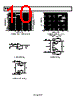
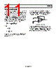
11 / 16 page 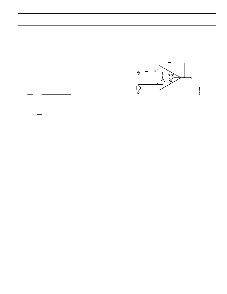 AD8392 Rev. 0 | Page 11 of 16 THEORY OF OPERATION The AD8392 is a current feedback amplifier with high (400 mA) output current capability. With a current feedback amplifier, the current into the inverting input is the feedback signal, and the open-loop behavior is that of a transimpedance, dVO/dIIN or TZ. The open-loop transimpedance is analogous to the open-loop voltage gain of a voltage feedback amplifier. Figure 33 shows a simplified model of a current feedback amplifier. Since RIN is proportional to 1/gm, the equivalent voltage gain is just TZ × gm, where gm is the transconductance of the input stage. Basic analysis of the follower with gain circuit yields () () F IN Z Z IN O R R G S T S T G V V + × + × = where: G F R R G + = 1 Ω 50 1 ≈ = m IN g R Since G × RIN << RF for low gains, a current feedback amplifier has relatively constant bandwidth versus gain, the 3 dB point being set when |TZ| = RF. Of course, for a real amplifier there are additional poles that contribute excess phase, and there is a value for RF below which the amplifier is unstable. Tolerance for peaking and desired flatness determines the optimum RF in each application. RF VOUT RG RN VIN RIN IIN TZ Figure 33. Simplified Block Diagram The AD8392 is capable of delivering 400 mA of output current while swinging to within 2 V of either power supply rail. The AD8392 also has a power management system included on-chip. It features four user-programmable power levels (three active power modes as well as the provision for complete shutdown). |
|
|
Link URL |
| Does ALLDATASHEET help your business so far? [ DONATE ] |
About Alldatasheet | Advertisement | Contact us | Privacy Policy | Link to Datasheet | Link Exchange | Manufacturer List All Rights Reserved©Alldatasheet.com |
| Russian : Alldatasheetru.com | Korean : Alldatasheet.co.kr | Spanish : Alldatasheet.es | French : Alldatasheet.fr | Italian : Alldatasheetit.com Portuguese : Alldatasheetpt.com | Polish : Alldatasheet.pl | Vietnamese : Alldatasheet.vn Indian : Alldatasheet.in | Mexican : Alldatasheet.com.mx | British : Alldatasheet.co.uk | New Zealand : Alldatasheet.co.nz |
|
Family Site : ic2ic.com |
icmetro.com |
 New Zealand ▼
 English
 Chinese
 German
 Japanese
 Russian
 Korean
 Spanish
 French
 Italian
 Portuguese
 Polish
 Vietnamese
 Indian
 Mexican
 British
 New Zealand