|
Electronic Components Datasheet Search |
|
|
Electronic Components Datasheet Search |
|
AD8139ACP-R2 Datasheet(PDF) 20 Page - Analog Devices |
|
|
|||||||||||||||||||||||||||||
AD8139ACP-R2 Datasheet(HTML) 20 Page - Analog Devices |
|
|
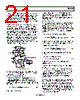
20 / 24 page 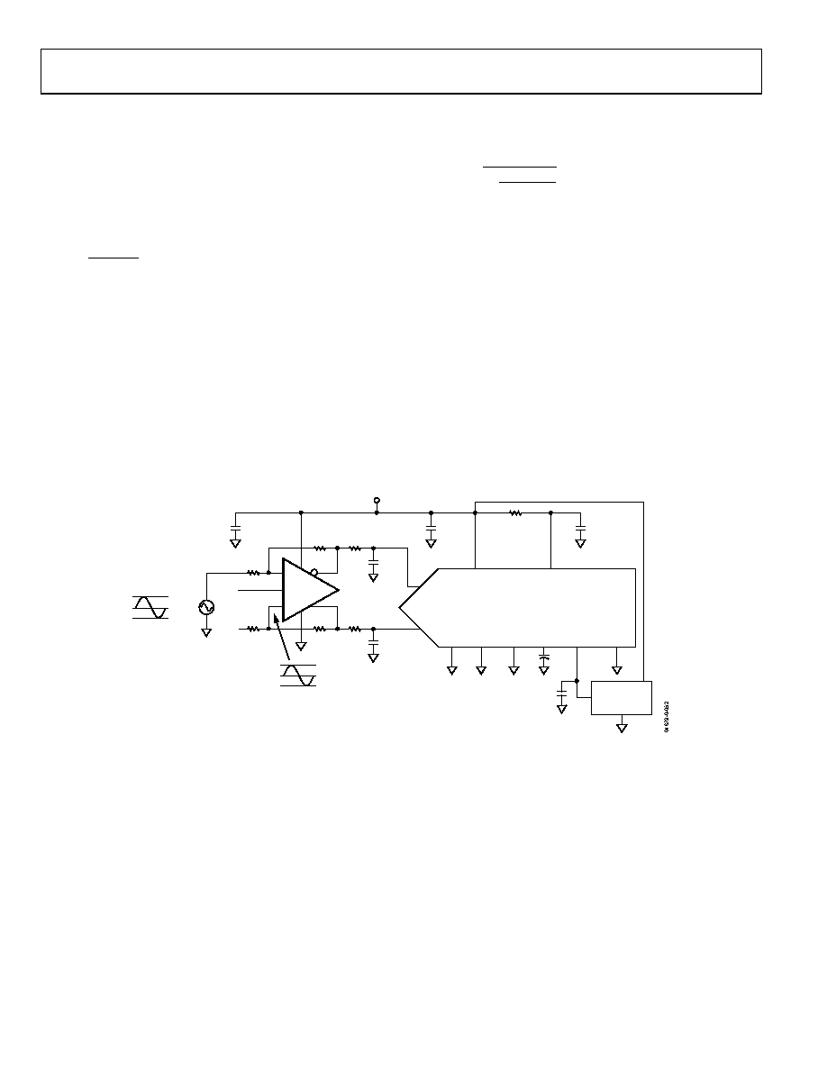 AD8139 Rev. A | Page 20 of 24 Using the β notation, Equation 15 can be written as ( ) ICM OCM ACM V V V β − + β = 1 (16) or equivalently, ( ) ICM OCM ICM ACM V V V V − β + = (17) where VICM is the common-mode voltage of the input signal, i.e., 2 IN IP ICM V V V + = . For proper operation, the voltages at VAN and VAP must stay within their respective linear ranges. Calculating Input Impedance The input impedance of the circuit in Figure 57 will depend on whether the amplifier is being driven by a single-ended or a differential signal source. For balanced differential input signals, the differential input impedance (RIN, dm) is simply G dm IN, R R 2 = (18) For a single-ended signal (for example, when VIN is grounded and the input signal drives VIP), the input impedance becomes ) ( 2 1 F G F G IN R R R R R + − = (19) The input impedance of a conventional inverting op amp configuration is simply RG, but it is higher in Equation 19 because a fraction of the differential output voltage appears at the summing junctions, VAN and VAP. This voltage partially bootstraps the voltage across the input resistor RG, leading to the increased input resistance. Input Common-Mode Swing Considerations In some single-ended-to-differential applications, when using a single-supply voltage attention must be paid to the swing of the input common-mode voltage, VACM. Consider the case in Figure 59, where VIN is 5 V p-p swinging about a baseline at ground and VREF is connected to ground. DGND AGND REFGND REF REFBUFIN PDBUF ADR431 2.5V REFERENCE 47 µF AD7674 IN+ IN– AVDD DVDD AD8139 + – 8 VREF 2.5V 2 1 6 3 4 5 VOCM 200 Ω 200 Ω 324 Ω 324 Ω 5V 20 Ω 15 Ω 15 Ω VIN 2.7nF 2.7nF 0.1 µF 0.1 µF 0.1 µF 0.1 µF +1.7V +0.95V VACM WITH VREF = 0 +0.2V +2.5V GND –2.5V Figure 59. AD8139 Driving AD7674, 18-Bit, 800 kSPS A/D Converter |
|
|
Link URL |
| Does ALLDATASHEET help your business so far? [ DONATE ] |
About Alldatasheet | Advertisement | Contact us | Privacy Policy | Link to Datasheet | Link Exchange | Manufacturer List All Rights Reserved©Alldatasheet.com |
| Russian : Alldatasheetru.com | Korean : Alldatasheet.co.kr | Spanish : Alldatasheet.es | French : Alldatasheet.fr | Italian : Alldatasheetit.com Portuguese : Alldatasheetpt.com | Polish : Alldatasheet.pl | Vietnamese : Alldatasheet.vn Indian : Alldatasheet.in | Mexican : Alldatasheet.com.mx | British : Alldatasheet.co.uk | New Zealand : Alldatasheet.co.nz |
|
Family Site : ic2ic.com |
icmetro.com |
 New Zealand ▼
 English
 Chinese
 German
 Japanese
 Russian
 Korean
 Spanish
 French
 Italian
 Portuguese
 Polish
 Vietnamese
 Indian
 Mexican
 British
 New Zealand