 |
Electronic Components Datasheet Search |
|
|
Electronic Components Datasheet Search |
|
ADRF5730BCCZN-R7 Datasheet(PDF) 13 Page - Analog Devices |
|
|
|||||||||||||||||||||||||||||
ADRF5730BCCZN-R7 Datasheet(HTML) 13 Page - Analog Devices |
|
|
13 / 19 page 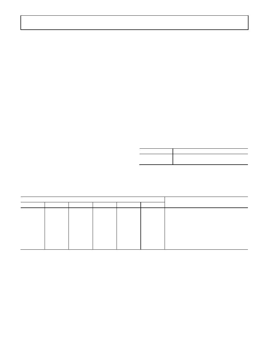 Data Sheet ADRF5730 Rev. 0 | Page 13 of 19 THEORY OF OPERATION The ADRF5730 incorporates a 6-bit fixed attenuator array that offers an attenuation range of 31.5 dB in 0.5 dB steps. An integrated driver provides both serial and parallel mode control of the attenuator array (see Figure 32). Note that when referring to a single function of a multifunction pin in this section, only the portion of the pin name that is relevant is mentioned. For full pin names of the multifunction pins, refer to the Pin Configuration and Function Descriptions section. POWER SUPPLY The ADRF5730 requires a positive supply voltage applied to the VDD pin and a negative supply voltage applied to the VSS pin. Bypassing capacitors are recommended on the supply lines to filter high frequency noise. The power-up sequence is as follows: 1. Connect GND. 2. Power up VDD. 3. Power up VSS. 4. Apply the digital control inputs. The relative order of the digital control inputs is not important. However, powering the digital control inputs before the VDD supply can inadvertently forward bias and damage the internal ESD protection structures. 5. Apply an RF input signal to ATTIN or ATTOUT. The power-down sequence is the reverse order of the power-up sequence. RF INPUT AND OUTPUT Both RF ports (ATTIN and ATTOUT) are dc-coupled to 0 V. No dc blocking is required at the RF ports when the RF line potential is equal to 0 V. The RF ports are internally matched to 50 Ω. Therefore, external matching components are not required. For wideband applications, use impedance matching to improve insertion loss, return loss, and attenuation accuracy performance at high frequencies. See the Impedance Matching section. The ADRF5730 supports bidirectional operation at a lower power level. The power handling of the ATTIN and ATTOUT ports are different. Therefore, the bidirectional power handling is defined by the ATTOUT port. Refer to the RF input power specifications in Table 1. SERIAL OR PARALLEL MODE SELECTION The ADRF5730 can be controlled in either serial or parallel mode by setting the PS pin to high or low, respectively (see Table 6). Table 6. Mode Selection PS Control Mode Low Parallel High Serial Table 7. Truth Table Digital Control Input1 Attenuation State (dB) D5 D4 D3 D2 D1 D0 Low Low Low Low Low Low 0 (reference) Low Low Low Low Low High 0.5 Low Low Low Low High Low 1.0 Low Low Low High Low Low 2.0 Low Low High Low Low Low 4.0 Low High Low Low Low Low 8.0 High Low Low Low Low Low 16.0 High High High High High High 31.5 1 Any combination of the control voltage input states shown in Table 7 provides an attenuation equal to the sum of the bits selected. |
|
|
Link URL |
| Does ALLDATASHEET help your business so far? [ DONATE ] |
About Alldatasheet | Advertisement | Contact us | Privacy Policy | Link to Datasheet | Link Exchange | Manufacturer List All Rights Reserved©Alldatasheet.com |
| Russian : Alldatasheetru.com | Korean : Alldatasheet.co.kr | Spanish : Alldatasheet.es | French : Alldatasheet.fr | Italian : Alldatasheetit.com Portuguese : Alldatasheetpt.com | Polish : Alldatasheet.pl | Vietnamese : Alldatasheet.vn Indian : Alldatasheet.in | Mexican : Alldatasheet.com.mx | British : Alldatasheet.co.uk | New Zealand : Alldatasheet.co.nz |
|
Family Site : ic2ic.com |
icmetro.com |
 New Zealand ▼
 English
 Chinese
 German
 Japanese
 Russian
 Korean
 Spanish
 French
 Italian
 Portuguese
 Polish
 Vietnamese
 Indian
 Mexican
 British
 New Zealand


