|
Electronic Components Datasheet Search |
|
|
Electronic Components Datasheet Search |
|
M95512-R Datasheet(PDF) 19 Page - STMicroelectronics |
|
|
|||||||||||||||||||||||||||||
M95512-R Datasheet(HTML) 19 Page - STMicroelectronics |
|
|
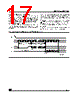
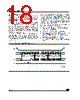
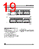
19 / 31 page 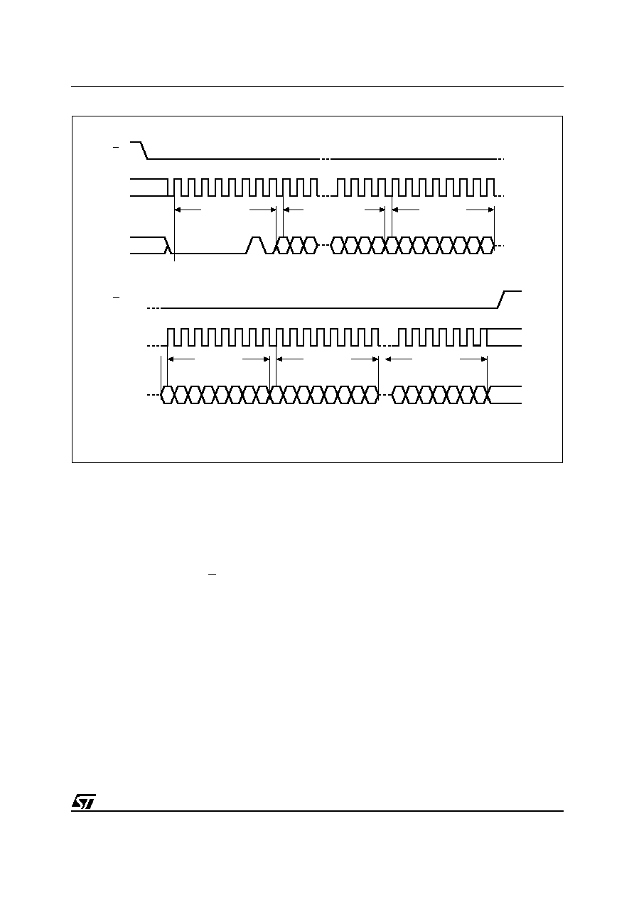 19/31 M95512-W, M95512-R Figure 14. Page Write (WRITE) Sequence POWER-UP AND DELIVERY STATE Power-up State After Power-up, the device is in the following state: – Standby Power mode – Deselected (after Power-up, a falling edge is required on Chip Select (S) before any instructions can be started). – Not in the Hold Condition – Write Enable Latch (WEL) is reset to 0 – Write In Progress (WIP) is reset to 0 The SRWD, BP1 and BP0 bits of the Status Reg- ister are unchanged from the previous power- down (they are non-volatile bits). Initial Delivery State The device is delivered with the memory array set at all 1s (FFh). The Status Register Write Disable (SRWD) and Block Protect (BP1 and BP0) bits are initialized to 0. C D AI01796D S 34 33 35 36 37 38 39 40 41 42 44 45 46 47 32 C D S 15 2 1 3456789 10 20 21 22 23 24 25 26 27 14 13 3210 28 29 30 Instruction 16-Bit Address 0 765432 0 1 Data Byte 1 31 43 765432 0 1 Data Byte 2 765432 0 1 Data Byte 3 65432 0 1 Data Byte N |
|
Link URL |
| Does ALLDATASHEET help your business so far? [ DONATE ] |
About Alldatasheet | Advertisement | Contact us | Privacy Policy | Link to Datasheet | Link Exchange | Manufacturer List All Rights Reserved©Alldatasheet.com |
| Russian : Alldatasheetru.com | Korean : Alldatasheet.co.kr | Spanish : Alldatasheet.es | French : Alldatasheet.fr | Italian : Alldatasheetit.com Portuguese : Alldatasheetpt.com | Polish : Alldatasheet.pl | Vietnamese : Alldatasheet.vn Indian : Alldatasheet.in | Mexican : Alldatasheet.com.mx | British : Alldatasheet.co.uk | New Zealand : Alldatasheet.co.nz |
|
Family Site : ic2ic.com |
icmetro.com |
 New Zealand ▼
 English
 Chinese
 German
 Japanese
 Russian
 Korean
 Spanish
 French
 Italian
 Portuguese
 Polish
 Vietnamese
 Indian
 Mexican
 British
 New Zealand