|
Electronic Components Datasheet Search |
|
|
Electronic Components Datasheet Search |
|
IS25LP064A-RBLE1 Datasheet(PDF) 18 Page - Integrated Silicon Solution, Inc |
|
|
|||||||||||||||||||||||||||||
IS25LP064A-RBLE1 Datasheet(HTML) 18 Page - Integrated Silicon Solution, Inc |
|
|
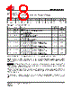
18 / 99 page 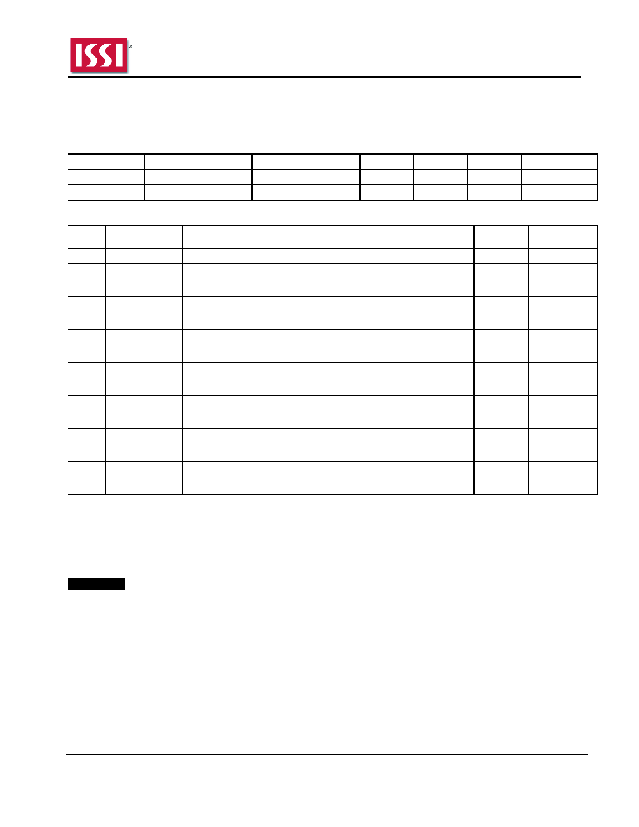 IS25LP064A/032A Integrated Silicon Solution, Inc.- www.issi.com 18 Rev. A 11/06/2015 6.2 FUNCTION REGISTER Function Register Format and Bit definition are described in Table 6.5 and Table 6.6. Table 6.5 Function Register Format Bit 7 Bit 6 Bit 5 Bit 4 Bit 3 Bit 2 Bit 1 Bit 0 IRL3 IRL2 IRL1 IRL0 ESUS PSUS TBS Reserved Default 0 0 0 0 0 0 0 0 Table 6.6 Function Register Bit Definition Bit Name Definition Read- /Write Type Bit 0 Reserved Reserved R Reserved Bit 1 Top/Bottom Selection Top/Bottom Selection. (See Table 6.4 for details) “0” indicates Top area. “1” indicates Bottom area. R/W OTP Bit 2 PSUS Program suspend bit: “0” indicates program is not suspend “1” indicates program is suspend R Volatile Bit 3 ESUS Erase suspend bit: "0" indicates Erase is not suspend "1" indicates Erase is suspend R Volatile Bit 4 IR Lock 0 Lock the Information Row 0: “0” indicates the Information Row can be programmed “1” indicates the Information Row cannot be programmed R/W OTP Bit 5 IR Lock 1 Lock the Information Row 1: “0” indicates the Information Row can be programmed “1” indicates the Information Row cannot be programmed R/W OTP Bit 6 IR Lock 2 Lock the Information Row 2: “0” indicates the Information Row can be programmed “1” indicates the Information Row cannot be programmed R/W OTP Bit 7 IR Lock 3 Lock the Information Row 3: “0” indicates the Information Row can be programmed “1” indicates the Information Row cannot be programmed R/W OTP Note: Once OTP bits of Function Register are written to “1”, it cannot be modified to “0” any more. Top/Bottom Selection: BP0~3 area assignment can be changed from Top (default) to Bottom by setting TBS bit to “1”. However, once Bottom is selected, it cannot be changed back to Top since TBS bit is OTP. See Table 6.4 for details The Program Suspend Status bit indicates when a Program operation has been suspended. The PSUS changes to “1” after a suspend command is issued during the program operation. Once the suspended Program resumes, the PSUS bit is reset to “0”. ESUS bit: The Erase Suspend Status indicates when an Erase operation has been suspended. The ESUS bit is “1” after a suspend command is issued during an Erase operation. Once the suspended Erase resumes, the ESUS bit is reset to “0”. IR Lock bit 0 ~ 3: The default is “0” so that the Information Row can be programmed. If the bit set to “1”, the Information Row can ’t be programmed. Once it set to “1”, it cannot be changed back to “0” since IR Lock bits are OTP. |
|
Link URL |
| Does ALLDATASHEET help your business so far? [ DONATE ] |
About Alldatasheet | Advertisement | Contact us | Privacy Policy | Link to Datasheet | Link Exchange | Manufacturer List All Rights Reserved©Alldatasheet.com |
| Russian : Alldatasheetru.com | Korean : Alldatasheet.co.kr | Spanish : Alldatasheet.es | French : Alldatasheet.fr | Italian : Alldatasheetit.com Portuguese : Alldatasheetpt.com | Polish : Alldatasheet.pl | Vietnamese : Alldatasheet.vn Indian : Alldatasheet.in | Mexican : Alldatasheet.com.mx | British : Alldatasheet.co.uk | New Zealand : Alldatasheet.co.nz |
|
Family Site : ic2ic.com |
icmetro.com |
 New Zealand ▼
 English
 Chinese
 German
 Japanese
 Russian
 Korean
 Spanish
 French
 Italian
 Portuguese
 Polish
 Vietnamese
 Indian
 Mexican
 British
 New Zealand