|
Electronic Components Datasheet Search |
|
|
Electronic Components Datasheet Search |
|
IS25LP064A-RGLA3 Datasheet(PDF) 66 Page - Integrated Silicon Solution, Inc |
|
|
|||||||||||||||||||||||||||||
IS25LP064A-RGLA3 Datasheet(HTML) 66 Page - Integrated Silicon Solution, Inc |
|
|
66 / 99 page 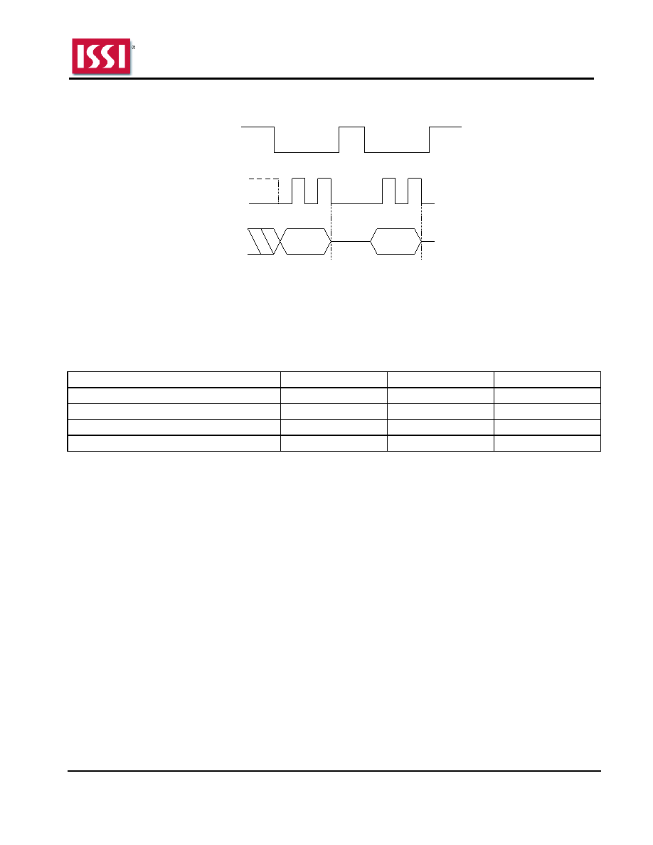 IS25LP064A/032A Integrated Silicon Solution, Inc.- www.issi.com 66 Rev. A 11/06/2015 Figure 8.51 Software Reset Enable and Software Reset QPI Sequence (RSTEN, 66h + RST, 99h) 66h CE# SCK IO[3:0] 0 1 Mode 3 Mode 0 99h 0 1 8.32 SECURITY INFORMATION ROW The security Information Row is comprised of an additional 4 x 256 bytes of programmable information. The security bits can be reprogrammed by the user. Any program security instruction issued while an erase, program or write cycle is in progress is rejected without having any effect on the cycle that is in progress. Table 8.7 Information Row Valid Address Range Address Assignment A[23:16] A[15:8] A[7:0] IRL0 (Information Row Lock0) 00h 00h Byte address IRL1 00h 10h Byte address IRL2 00h 20h Byte address IRL3 00h 30h Byte address Bit 7~4 of the Function Register is used to permanently lock the programmable memory array. When Function Register bit IRLx = “0”, the 256 bytes of the programmable memory array can be programmed. When Function Register bit IRLx = “1”, the 256 bytes of the programmable memory array function as read only. |
|
Link URL |
| Does ALLDATASHEET help your business so far? [ DONATE ] |
About Alldatasheet | Advertisement | Contact us | Privacy Policy | Link to Datasheet | Link Exchange | Manufacturer List All Rights Reserved©Alldatasheet.com |
| Russian : Alldatasheetru.com | Korean : Alldatasheet.co.kr | Spanish : Alldatasheet.es | French : Alldatasheet.fr | Italian : Alldatasheetit.com Portuguese : Alldatasheetpt.com | Polish : Alldatasheet.pl | Vietnamese : Alldatasheet.vn Indian : Alldatasheet.in | Mexican : Alldatasheet.com.mx | British : Alldatasheet.co.uk | New Zealand : Alldatasheet.co.nz |
|
Family Site : ic2ic.com |
icmetro.com |
 New Zealand ▼
 English
 Chinese
 German
 Japanese
 Russian
 Korean
 Spanish
 French
 Italian
 Portuguese
 Polish
 Vietnamese
 Indian
 Mexican
 British
 New Zealand