 |
Electronic Components Datasheet Search |
|
|
Electronic Components Datasheet Search |
|
ADP322ACPZ-189-R7 Datasheet(PDF) 21 Page - Analog Devices |
|
|
|||||||||||||||||||||||||||||
ADP322ACPZ-189-R7 Datasheet(HTML) 21 Page - Analog Devices |
|
|
21 / 24 page 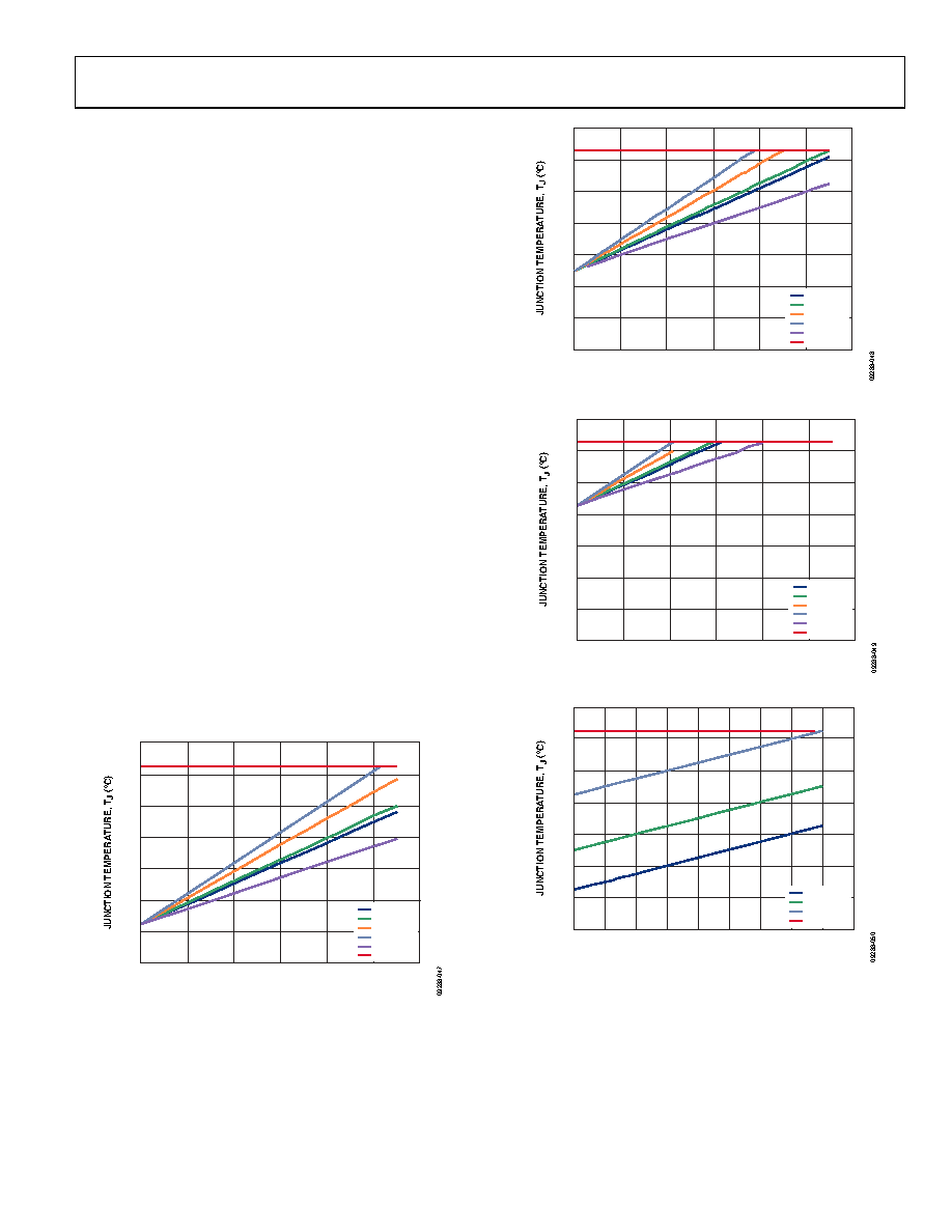 Data Sheet ADP322/ADP323 Rev. E | Page 21 of 24 The junction temperature of the ADP322/ADP323 can be calculated from the following equation: TJ = TA + (PD × θJA) (2) where: TA is the ambient temperature. PD is the power dissipation in the die, given by PD = Σ[(VIN − VOUT) × ILOAD] + Σ(VIN × IGND) (3) where: ILOAD is the load current. IGND is the ground current. VIN and VOUT are input and output voltages, respectively. Power dissipation due to ground current is quite small and can be ignored. Therefore, the junction temperature equation simplifies to TJ = TA + {Σ[(VIN − VOUT) × ILOAD] × θJA} (4) As shown in Equation 4, for a given ambient temperature, input to output voltage differential, and continuous load current, there exists a minimum copper size requirement for the PCB to ensure that the junction temperature does not rise above 125°C. Figure 58 to Figure 61 show junction temperature calculations for different ambient temperatures, total power dissipation, and areas of PCB copper. In cases where the board temperature is known, the thermal characterization parameter, ΨJB, can be used to estimate the junction temperature rise. TJ is calculated from TB and PD using the formula TJ = TB + (PD × ΨJB) (5) The typical ΨJB value for the 16-lead, 3 mm × 3 mm LFCSP is 25.2°C/W. 0 20 40 60 80 100 120 140 0 0.2 0.4 0.6 0.8 1.0 1.2 TOTAL POWER DISSIPATION (W) 1000mm2 500mm2 100mm2 50mm2 JEDEC TJ MAX Figure 58. Junction Temperature vs. Total Power Dissipation, TA = 25°C 0 20 40 60 80 100 120 140 0 0.2 0.4 0.6 0.8 1.0 1.2 TOTAL POWER DISSIPATION (W) 1000mm2 500mm2 100mm2 50mm2 JEDEC TJ MAX Figure 59. Junction Temperature vs. Total Power Dissipation, TA = 50°C 0 20 40 60 80 100 120 140 0 0.2 0.4 0.6 0.8 1.0 1.2 TOTAL POWER DISSIPATION (W) 1000mm2 500mm2 100mm2 50mm2 JEDEC TJ MAX Figure 60. Junction Temperature vs. Total Power Dissipation, TA = 85°C 0 20 40 60 80 100 120 140 0 0.2 0.4 0.6 0.8 1.0 1.2 1.4 1.6 1.8 TOTAL POWER DISSIPATION (W) TB = 25°C TB = 50°C TB = 85°C TJ MAX Figure 61. Junction Temperature vs. Total Power Dissipation and Board Temperature |
|
|
Link URL |
| Does ALLDATASHEET help your business so far? [ DONATE ] |
About Alldatasheet | Advertisement | Contact us | Privacy Policy | Link to Datasheet | Link Exchange | Manufacturer List All Rights Reserved©Alldatasheet.com |
| Russian : Alldatasheetru.com | Korean : Alldatasheet.co.kr | Spanish : Alldatasheet.es | French : Alldatasheet.fr | Italian : Alldatasheetit.com Portuguese : Alldatasheetpt.com | Polish : Alldatasheet.pl | Vietnamese : Alldatasheet.vn Indian : Alldatasheet.in | Mexican : Alldatasheet.com.mx | British : Alldatasheet.co.uk | New Zealand : Alldatasheet.co.nz |
|
Family Site : ic2ic.com |
icmetro.com |
 New Zealand ▼
 English
 Chinese
 German
 Japanese
 Russian
 Korean
 Spanish
 French
 Italian
 Portuguese
 Polish
 Vietnamese
 Indian
 Mexican
 British
 New Zealand


