|
Electronic Components Datasheet Search |
|
|
Electronic Components Datasheet Search |
|
25AA320A Datasheet(PDF) 11 Page - Microchip Technology |
|
|
|||||||||||||||||||||||||||||
25AA320A Datasheet(HTML) 11 Page - Microchip Technology |
|
|
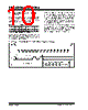
11 / 26 page  © 2007 Microchip Technology Inc. DS21828C-page 11 25AA320A/25LC320A 2.6 Write Status Register Instruction (WRSR) The Write Status Register instruction (WRSR) allows the user to write to the nonvolatile bits in the STATUS register as shown in Table 2-2. The user is able to select one of four levels of protection for the array by writing to the appropriate bits in the STATUS register. The array is divided up into four segments. The user has the ability to write-protect none, one, two or all four of the segments of the array. The partitioning is controlled as shown in Table 2-3. The Write-Protect Enable (WPEN) bit is a nonvolatile bit that is available as an enable bit for the WP pin. The Write-Protect (WP) pin and the Write-Protect Enable (WPEN) bit in the STATUS register control the programmable hardware write-protect feature. Hard- ware write protection is enabled when WP pin is low and the WPEN bit is high. Hardware write protection is disabled when either the WP pin is high or the WPEN bit is low. When the chip is hardware write-protected, only writes to nonvolatile bits in the STATUS register are disabled. See Table 2-4 for a matrix of functionality on the WPEN bit. See Figure 2-7 for the WRSR timing sequence. TABLE 2-3: ARRAY PROTECTION FIGURE 2-7: WRITE STATUS REGISTER TIMING SEQUENCE (WRSR) BP1 BP0 Array Addresses Write-Protected 00 none 01 upper 1/4 (0C00h - 0FFFh) 10 upper 1/2 (0800h - 0FFFh) 11 all (0000h - 0FFFh) SO SI CS 9 1011 12131415 0 1 0 0 0 0 00 76 5 4 21 0 Instruction Data to STATUS Register High-Impedance SCK 0 2 34 56 7 1 8 3 Note: An internal write cycle (TWC) is initiated on the rising edge of CS after a valid write STATUS register sequence. |
|
|
Link URL |
| Does ALLDATASHEET help your business so far? [ DONATE ] |
About Alldatasheet | Advertisement | Contact us | Privacy Policy | Link to Datasheet | Link Exchange | Manufacturer List All Rights Reserved©Alldatasheet.com |
| Russian : Alldatasheetru.com | Korean : Alldatasheet.co.kr | Spanish : Alldatasheet.es | French : Alldatasheet.fr | Italian : Alldatasheetit.com Portuguese : Alldatasheetpt.com | Polish : Alldatasheet.pl | Vietnamese : Alldatasheet.vn Indian : Alldatasheet.in | Mexican : Alldatasheet.com.mx | British : Alldatasheet.co.uk | New Zealand : Alldatasheet.co.nz |
|
Family Site : ic2ic.com |
icmetro.com |
 New Zealand ▼
 English
 Chinese
 German
 Japanese
 Russian
 Korean
 Spanish
 French
 Italian
 Portuguese
 Polish
 Vietnamese
 Indian
 Mexican
 British
 New Zealand