 |
Electronic Components Datasheet Search |
|
|
Electronic Components Datasheet Search |
|
FLIPSTACKCSP Datasheet(PDF) 2 Page - Amkor Technology |
|
|
|||||||||||||||||||||||||||||
FLIPSTACKCSP Datasheet(HTML) 2 Page - Amkor Technology |
|
|
2 / 2 page 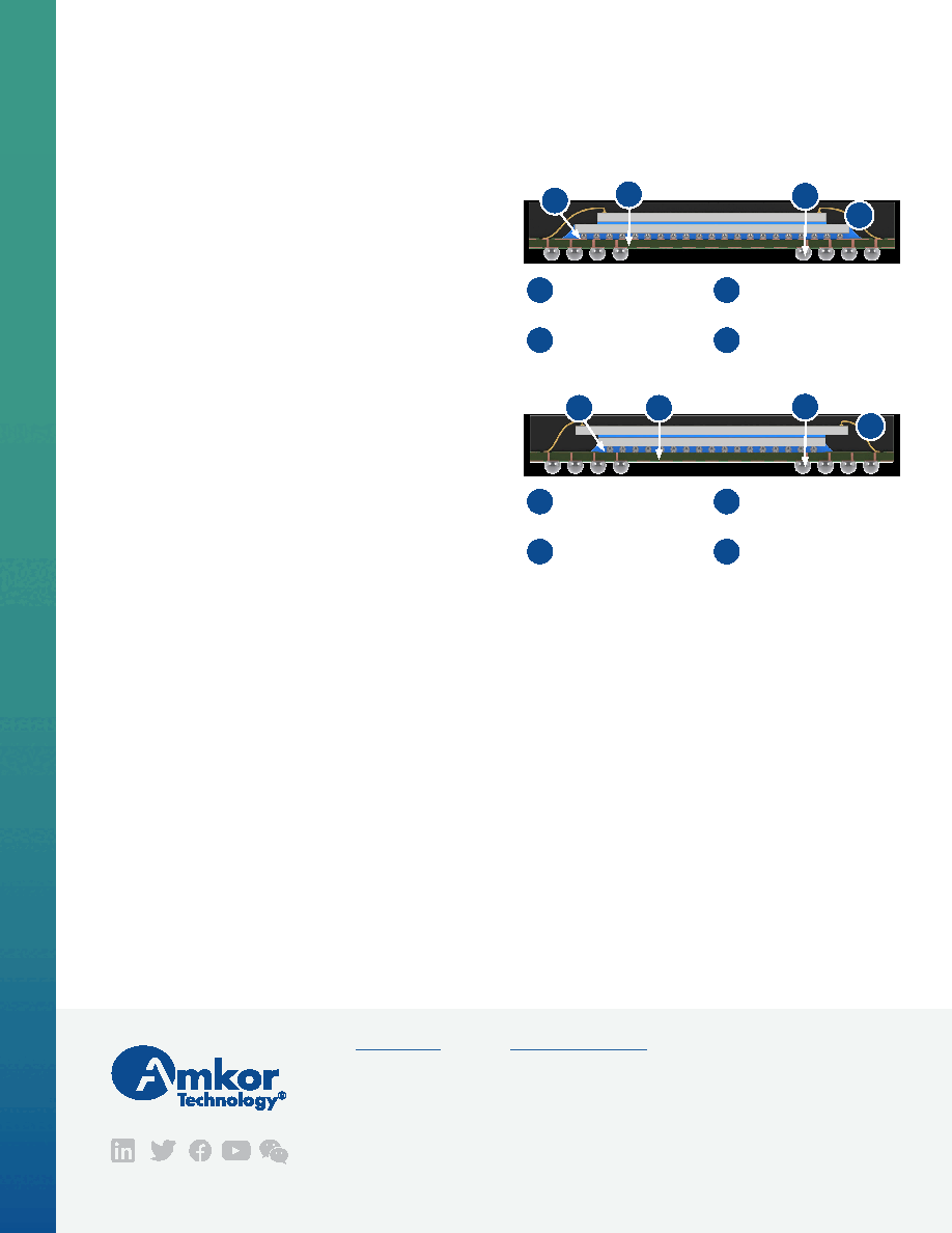 With respect to the information in this document, Amkor makes no guarantee or warranty of its accuracy or that the use of such information will not infringe upon the intellectual rights of third parties. Amkor shall not be responsible for any loss or damage of whatever nature resulting from the use of, or reliance upon it and no patent or other license is implied hereby. This document does not in any way extend or modify Amkor’s warranty on any product beyond that set forth in its standard terms and conditions of sale. Amkor reserves the right to make changes in its product and specifications at any time and without notice. The Amkor name and logo are registered trademarks of Amkor Technology, Inc. All other trademarks mentioned are property of their respective companies. © 2019 Amkor Technology, Incorporated. All Rights Reserved. DS820D-EN Rev Date: 09/19 Visit amkor.com or email sales@amkor.com for more information. Process Highlights f Ball pad pitch: 0.35, 0.4, 0.5, 0.65, 0.75, 0.8, 1.0 mm f Die thickness (flip chip): As thin as 70 μm f Die thickness (wirebond): As thin as 50 μm f Ball diameter: As required f Wirebond pitch (min): 40 μm in-line with roadmap to 25 μm f Bump pitch mass reflow: 60 μm in-line f Thermal compression: 50 μm in-line f Wirebond length (max): 5 mm (200 mils) f Wirebond diameter (min): 0.7, 0.8, 0.9, 1.0 mil+ in gold, silver or copper wirebond diameters f Wafer diameter: 150, 200 & 300 mm wafers FlipStack® CSP Cross Sections Standard Materials f Package substrate ▷ Laminate dielectric ⨠ HL832: NXA, NS, NS-LC, NSF-LCA ⨠ E679: FG, FGB, FGBS, GT, E700G, E705G, DS7409HG, DS7409HGB(S), DS7409HGB(LE), ELC4785GSB, ELC4785THB, ELC4785THG ▷ Layer count (laminate): 2-6 f Die attach ▷ Bottom die: Flip chip attached by mass reflow or thermal compression ▷ Top die: Non-conductive epoxy, film f Wire type: Au, Cu or Ag f Encapsulant: Transfer molded epoxy f Underfill: Capillary or molded f Bumps (F/C die): Pb-free, eutectic, Cu pillar f Solder balls: Pb-free, eutectic f Device type: Silicon, SiGe, GaAs, glass (IPD film on glass) f Marking: Laser Capillary or molded underfill options 2-6 Layer substrates A B C Eutectic or lead-free solder ball options Gold, silver or copper wire options D Capillary or molded underfill options 2-6 Layer substrates A B C Eutectic or lead-free solder ball options Gold, silver or copper wire options D D A B C D A B C |
|
|
Link URL |
| Does ALLDATASHEET help your business so far? [ DONATE ] |
About Alldatasheet | Advertisement | Contact us | Privacy Policy | Link to Datasheet | Link Exchange | Manufacturer List All Rights Reserved©Alldatasheet.com |
| Russian : Alldatasheetru.com | Korean : Alldatasheet.co.kr | Spanish : Alldatasheet.es | French : Alldatasheet.fr | Italian : Alldatasheetit.com Portuguese : Alldatasheetpt.com | Polish : Alldatasheet.pl | Vietnamese : Alldatasheet.vn Indian : Alldatasheet.in | Mexican : Alldatasheet.com.mx | British : Alldatasheet.co.uk | New Zealand : Alldatasheet.co.nz |
|
Family Site : ic2ic.com |
icmetro.com |
 New Zealand ▼
 English
 Chinese
 German
 Japanese
 Russian
 Korean
 Spanish
 French
 Italian
 Portuguese
 Polish
 Vietnamese
 Indian
 Mexican
 British
 New Zealand


